
Preface
Caveat
IMPORTANT: This document focuses at the moment on
1st and 2nd generation devices (models before the Game
Boy Color), and some hardware details are very different
in later generations.
Be very careful if you make assumptions about later gen-
eration devices based on this document!
2

How to read this document
🧩 Speculation
This is something that hasn’t been verified, but would make a lot of sense.
Caveat
This explains some caveat about this documentation that you should know.
Warning
This is a warning about something.
0.1 Formatting of numbers
When a single bit is discussed in isolation, the value looks like this: 0, 1.
Binary numbers are prefixed with 0b like this: 0b0101101, 0b11011, 0b00000000. Values are pre-
fixed with zeroes when necessary, so the total number of digits always matches the number of
digits in the value.
Hexadecimal numbers are prefixed with 0x like this: 0x1234, 0xDEADBEEF, 0xFF04. Values are
prefixed with zeroes when necessary, so the total number of characters always matches the
number of nibbles in the value.
Examples:
4-bit 8-bit 16-bit
Binary
0b0101 0b10100101 0b0000101010100101
Hexadecimal
0x5 0xA5 0x0AA5
3
0.2 Register definitions
Register0.1: 0x1234 - This is a hardware register definition
R/W-0 R/W-1 U-1 R-0 R-1 R-x W-1 U-0
VALUE<1:0> BIGVAL<7:5> FLAG
bit 7 6 5 4 3 2 1 bit 0
Top row legend:
R Bit can be read.
W Bit can be written. If the bit cannot be read, reading returns a constant value defined
in the bit list of the register in question.
U Unimplemented bit. Writing has no effect, and reading returns a constant value defined
in the bit list of the register in question.
-n Value after system reset: 0, 1, or x.
1
Bit is set.
0
Bit is cleared.
x Bit is unknown (e.g. depends on external things such as user input)
Middle row legend:
VALUE<1:0>
Bits 1 and 0 of VALUE
Unimplemented bit
BIGVAL<7:5>
Bits 7, 6, 5 of BIGVAL
FLAG
Single-bit value FLAG
In this example:
• After system reset, VALUE is 0b01, BIGVAL is either 0b010 or 0b011, FLAG is 0b1.
• Bits 5 and 0 are unimplemented. Bit 5 always returns 1, and bit 0 always returns 0.
• Both bits of VALUE can be read and written. When this register is written, bit 7 of the written
value goes to bit 1 of VALUE.
• FLAG can only be written to, so reads return a value that is defined elsewhere.
• BIGVAL cannot be written to. Only bits 5-7 of BIGVAL are defined here, so look elsewhere for
the low bits 0-4.
4
Contents
Preface . . . . . . . . . . . . . . . . . . . . . . . . . . . . . . . . . . . . . . . . . . . . . . . . . . . . . . . . . . . . . . . . . . . . . . . 2
How to read this document . . . . . . . . . . . . . . . . . . . . . . . . . . . . . . . . . . . . . . . . . . . . . . . . . . . . . 3
0.1 Formatting of numbers . . . . . . . . . . . . . . . . . . . . . . . . . . . . . . . . . . . . . . . . . . . . . . . . . . . . . . . . 3
0.2 Register definitions . . . . . . . . . . . . . . . . . . . . . . . . . . . . . . . . . . . . . . . . . . . . . . . . . . . . . . . . . . . . 4
Contents . . . . . . . . . . . . . . . . . . . . . . . . . . . . . . . . . . . . . . . . . . . . . . . . . . . . . . . . . . . . . . . . . . . . . . 5
I Game Boy console architecture . . . . . . . . . . . . . . . . . . . . . . . . . . . . . . . . . . . . . . . . . . . . . . . 10
1 Introduction . . . . . . . . . . . . . . . . . . . . . . . . . . . . . . . . . . . . . . . . . . . . . . . . . . . . . . . . . . . . . . . . 11
2 Clocks . . . . . . . . . . . . . . . . . . . . . . . . . . . . . . . . . . . . . . . . . . . . . . . . . . . . . . . . . . . . . . . . . . . . . 13
2.1 System clock . . . . . . . . . . . . . . . . . . . . . . . . . . . . . . . . . . . . . . . . . . . . . . . . . . . . . . . . . . . . . . . 13
System clock frequency . . . . . . . . . . . . . . . . . . . . . . . . . . . . . . . . . . . . . . . . . . . . . . . . . . . . . . . 13
2.2 Clock periods, T-cycles, and M-cycles . . . . . . . . . . . . . . . . . . . . . . . . . . . . . . . . . . . . . . . . . . 13
II Sharp SM83 CPU core . . . . . . . . . . . . . . . . . . . . . . . . . . . . . . . . . . . . . . . . . . . . . . . . . . . . . . . . 15
3 Introduction . . . . . . . . . . . . . . . . . . . . . . . . . . . . . . . . . . . . . . . . . . . . . . . . . . . . . . . . . . . . . . . . 16
3.1 History . . . . . . . . . . . . . . . . . . . . . . . . . . . . . . . . . . . . . . . . . . . . . . . . . . . . . . . . . . . . . . . . . . . . 16
4 Simple model . . . . . . . . . . . . . . . . . . . . . . . . . . . . . . . . . . . . . . . . . . . . . . . . . . . . . . . . . . . . . . . 17
5 CPU core timing . . . . . . . . . . . . . . . . . . . . . . . . . . . . . . . . . . . . . . . . . . . . . . . . . . . . . . . . . . . . . 18
5.1 Fetch/execute overlap . . . . . . . . . . . . . . . . . . . . . . . . . . . . . . . . . . . . . . . . . . . . . . . . . . . . . . . 18
Fetch/execute overlap timing example . . . . . . . . . . . . . . . . . . . . . . . . . . . . . . . . . . . . . . . . . . 18
6 Sharp SM83 instruction set . . . . . . . . . . . . . . . . . . . . . . . . . . . . . . . . . . . . . . . . . . . . . . . . . . . 20
6.1 Overview . . . . . . . . . . . . . . . . . . . . . . . . . . . . . . . . . . . . . . . . . . . . . . . . . . . . . . . . . . . . . . . . . . 20
CB opcode prefix . . . . . . . . . . . . . . . . . . . . . . . . . . . . . . . . . . . . . . . . . . . . . . . . . . . . . . . . . . . . 20
Undefined opcodes . . . . . . . . . . . . . . . . . . . . . . . . . . . . . . . . . . . . . . . . . . . . . . . . . . . . . . . . . . 20
6.2 8-bit load instructions . . . . . . . . . . . . . . . . . . . . . . . . . . . . . . . . . . . . . . . . . . . . . . . . . . . . . . . 21
LD r, r’: Load register (register) . . . . . . . . . . . . . . . . . . . . . . . . . . . . . . . . . . . . . . . . . . . . . . . . . 21
LD r, n: Load register (immediate) . . . . . . . . . . . . . . . . . . . . . . . . . . . . . . . . . . . . . . . . . . . . . . 22
LD r, (HL): Load register (indirect HL) . . . . . . . . . . . . . . . . . . . . . . . . . . . . . . . . . . . . . . . . . . . . 23
LD (HL), r: Load from register (indirect HL) . . . . . . . . . . . . . . . . . . . . . . . . . . . . . . . . . . . . . . . 24
LD (HL), n: Load from immediate data (indirect HL) . . . . . . . . . . . . . . . . . . . . . . . . . . . . . . . 25
LD A, (BC): Load accumulator (indirect BC) . . . . . . . . . . . . . . . . . . . . . . . . . . . . . . . . . . . . . . . 26
LD A, (DE): Load accumulator (indirect DE) . . . . . . . . . . . . . . . . . . . . . . . . . . . . . . . . . . . . . . . 27
LD (BC), A: Load from accumulator (indirect BC) . . . . . . . . . . . . . . . . . . . . . . . . . . . . . . . . . . 28
LD (DE), A: Load from accumulator (indirect DE) . . . . . . . . . . . . . . . . . . . . . . . . . . . . . . . . . . 29
LD A, (nn): Load accumulator (direct) . . . . . . . . . . . . . . . . . . . . . . . . . . . . . . . . . . . . . . . . . . . 30
LD (nn), A: Load from accumulator (direct) . . . . . . . . . . . . . . . . . . . . . . . . . . . . . . . . . . . . . . 31
LDH A, (C): Load accumulator (indirect 0xFF00+C) . . . . . . . . . . . . . . . . . . . . . . . . . . . . . . . . 32
LDH (C), A: Load from accumulator (indirect 0xFF00+C) . . . . . . . . . . . . . . . . . . . . . . . . . . . . 33
LDH A, (n): Load accumulator (direct 0xFF00+n) . . . . . . . . . . . . . . . . . . . . . . . . . . . . . . . . . . 34
LDH (n), A: Load from accumulator (direct 0xFF00+n) . . . . . . . . . . . . . . . . . . . . . . . . . . . . . 35
LD A, (HL-): Load accumulator (indirect HL, decrement) . . . . . . . . . . . . . . . . . . . . . . . . . . . 36
LD (HL-), A: Load from accumulator (indirect HL, decrement) . . . . . . . . . . . . . . . . . . . . . . . 37
LD A, (HL+): Load accumulator (indirect HL, increment) . . . . . . . . . . . . . . . . . . . . . . . . . . . . 38
LD (HL+), A: Load from accumulator (indirect HL, increment) . . . . . . . . . . . . . . . . . . . . . . . 39
6.3 16-bit load instructions . . . . . . . . . . . . . . . . . . . . . . . . . . . . . . . . . . . . . . . . . . . . . . . . . . . . . . 40
5
LD rr, nn: Load 16-bit register / register pair . . . . . . . . . . . . . . . . . . . . . . . . . . . . . . . . . . . . . 40
LD (nn), SP: Load from stack pointer (direct) . . . . . . . . . . . . . . . . . . . . . . . . . . . . . . . . . . . . . 41
LD SP, HL: Load stack pointer from HL . . . . . . . . . . . . . . . . . . . . . . . . . . . . . . . . . . . . . . . . . . 42
PUSH rr: Push to stack . . . . . . . . . . . . . . . . . . . . . . . . . . . . . . . . . . . . . . . . . . . . . . . . . . . . . . . . 43
POP rr: Pop from stack . . . . . . . . . . . . . . . . . . . . . . . . . . . . . . . . . . . . . . . . . . . . . . . . . . . . . . . 44
LD HL, SP+e: Load HL from adjusted stack pointer . . . . . . . . . . . . . . . . . . . . . . . . . . . . . . . . 45
6.4 8-bit arithmetic and logical instructions . . . . . . . . . . . . . . . . . . . . . . . . . . . . . . . . . . . . . . . 46
ADD r: Add (register) . . . . . . . . . . . . . . . . . . . . . . . . . . . . . . . . . . . . . . . . . . . . . . . . . . . . . . . . . 46
ADD (HL): Add (indirect HL) . . . . . . . . . . . . . . . . . . . . . . . . . . . . . . . . . . . . . . . . . . . . . . . . . . . . 47
ADD n: Add (immediate) . . . . . . . . . . . . . . . . . . . . . . . . . . . . . . . . . . . . . . . . . . . . . . . . . . . . . . 48
ADC r: Add with carry (register) . . . . . . . . . . . . . . . . . . . . . . . . . . . . . . . . . . . . . . . . . . . . . . . . 49
ADC (HL): Add with carry (indirect HL) . . . . . . . . . . . . . . . . . . . . . . . . . . . . . . . . . . . . . . . . . . . 50
ADC n: Add with carry (immediate) . . . . . . . . . . . . . . . . . . . . . . . . . . . . . . . . . . . . . . . . . . . . . 51
SUB r: Subtract (register) . . . . . . . . . . . . . . . . . . . . . . . . . . . . . . . . . . . . . . . . . . . . . . . . . . . . . . 52
SUB (HL): Subtract (indirect HL) . . . . . . . . . . . . . . . . . . . . . . . . . . . . . . . . . . . . . . . . . . . . . . . . 53
SUB n: Subtract (immediate) . . . . . . . . . . . . . . . . . . . . . . . . . . . . . . . . . . . . . . . . . . . . . . . . . . . 54
SBC r: Subtract with carry (register) . . . . . . . . . . . . . . . . . . . . . . . . . . . . . . . . . . . . . . . . . . . . 55
SBC (HL): Subtract with carry (indirect HL) . . . . . . . . . . . . . . . . . . . . . . . . . . . . . . . . . . . . . . . 56
SBC n: Subtract with carry (immediate) . . . . . . . . . . . . . . . . . . . . . . . . . . . . . . . . . . . . . . . . . 57
CP r: Compare (register) . . . . . . . . . . . . . . . . . . . . . . . . . . . . . . . . . . . . . . . . . . . . . . . . . . . . . . 58
CP (HL): Compare (indirect HL) . . . . . . . . . . . . . . . . . . . . . . . . . . . . . . . . . . . . . . . . . . . . . . . . . 59
CP n: Compare (immediate) . . . . . . . . . . . . . . . . . . . . . . . . . . . . . . . . . . . . . . . . . . . . . . . . . . . 60
INC r: Increment (register) . . . . . . . . . . . . . . . . . . . . . . . . . . . . . . . . . . . . . . . . . . . . . . . . . . . . 61
INC (HL): Increment (indirect HL) . . . . . . . . . . . . . . . . . . . . . . . . . . . . . . . . . . . . . . . . . . . . . . . 62
DEC r: Decrement (register) . . . . . . . . . . . . . . . . . . . . . . . . . . . . . . . . . . . . . . . . . . . . . . . . . . . 63
DEC (HL): Decrement (indirect HL) . . . . . . . . . . . . . . . . . . . . . . . . . . . . . . . . . . . . . . . . . . . . . . 64
AND r: Bitwise AND (register) . . . . . . . . . . . . . . . . . . . . . . . . . . . . . . . . . . . . . . . . . . . . . . . . . . 65
AND (HL): Bitwise AND (indirect HL) . . . . . . . . . . . . . . . . . . . . . . . . . . . . . . . . . . . . . . . . . . . . 66
AND n: Bitwise AND (immediate) . . . . . . . . . . . . . . . . . . . . . . . . . . . . . . . . . . . . . . . . . . . . . . . 67
OR r: Bitwise OR (register) . . . . . . . . . . . . . . . . . . . . . . . . . . . . . . . . . . . . . . . . . . . . . . . . . . . . . 68
OR (HL): Bitwise OR (indirect HL) . . . . . . . . . . . . . . . . . . . . . . . . . . . . . . . . . . . . . . . . . . . . . . . 69
OR n: Bitwise OR (immediate) . . . . . . . . . . . . . . . . . . . . . . . . . . . . . . . . . . . . . . . . . . . . . . . . . . 70
XOR r: Bitwise XOR (register) . . . . . . . . . . . . . . . . . . . . . . . . . . . . . . . . . . . . . . . . . . . . . . . . . . 71
XOR (HL): Bitwise XOR (indirect HL) . . . . . . . . . . . . . . . . . . . . . . . . . . . . . . . . . . . . . . . . . . . . . 72
XOR n: Bitwise XOR (immediate) . . . . . . . . . . . . . . . . . . . . . . . . . . . . . . . . . . . . . . . . . . . . . . . 73
CCF: Complement carry flag . . . . . . . . . . . . . . . . . . . . . . . . . . . . . . . . . . . . . . . . . . . . . . . . . . . 74
SCF: Set carry flag . . . . . . . . . . . . . . . . . . . . . . . . . . . . . . . . . . . . . . . . . . . . . . . . . . . . . . . . . . . . 75
DAA: Decimal adjust accumulator . . . . . . . . . . . . . . . . . . . . . . . . . . . . . . . . . . . . . . . . . . . . . . 76
CPL: Complement accumulator . . . . . . . . . . . . . . . . . . . . . . . . . . . . . . . . . . . . . . . . . . . . . . . . 77
6.5 16-bit arithmetic instructions . . . . . . . . . . . . . . . . . . . . . . . . . . . . . . . . . . . . . . . . . . . . . . . . . 78
INC rr: Increment 16-bit register . . . . . . . . . . . . . . . . . . . . . . . . . . . . . . . . . . . . . . . . . . . . . . . 78
DEC rr: Decrement 16-bit register . . . . . . . . . . . . . . . . . . . . . . . . . . . . . . . . . . . . . . . . . . . . . . 79
ADD HL, rr: Add (16-bit register) . . . . . . . . . . . . . . . . . . . . . . . . . . . . . . . . . . . . . . . . . . . . . . . 80
ADD SP, e: Add to stack pointer (relative) . . . . . . . . . . . . . . . . . . . . . . . . . . . . . . . . . . . . . . . . 81
6.6 Rotate, shift, and bit operation instructions . . . . . . . . . . . . . . . . . . . . . . . . . . . . . . . . . . . . 83
RLCA: Rotate left circular (accumulator) . . . . . . . . . . . . . . . . . . . . . . . . . . . . . . . . . . . . . . . . . 83
RRCA: Rotate right circular (accumulator) . . . . . . . . . . . . . . . . . . . . . . . . . . . . . . . . . . . . . . . 84
RLA: Rotate left (accumulator) . . . . . . . . . . . . . . . . . . . . . . . . . . . . . . . . . . . . . . . . . . . . . . . . . 85
RRA: Rotate right (accumulator) . . . . . . . . . . . . . . . . . . . . . . . . . . . . . . . . . . . . . . . . . . . . . . . . 86
6
RLC r: Rotate left circular (register) . . . . . . . . . . . . . . . . . . . . . . . . . . . . . . . . . . . . . . . . . . . . . 87
RLC (HL): Rotate left circular (indirect HL) . . . . . . . . . . . . . . . . . . . . . . . . . . . . . . . . . . . . . . . . 88
RRC r: Rotate right circular (register) . . . . . . . . . . . . . . . . . . . . . . . . . . . . . . . . . . . . . . . . . . . . 89
RRC (HL): Rotate right circular (indirect HL) . . . . . . . . . . . . . . . . . . . . . . . . . . . . . . . . . . . . . . 90
RL r: Rotate left (register) . . . . . . . . . . . . . . . . . . . . . . . . . . . . . . . . . . . . . . . . . . . . . . . . . . . . . 91
RL (HL): Rotate left (indirect HL) . . . . . . . . . . . . . . . . . . . . . . . . . . . . . . . . . . . . . . . . . . . . . . . . 92
RR r: Rotate right (register) . . . . . . . . . . . . . . . . . . . . . . . . . . . . . . . . . . . . . . . . . . . . . . . . . . . . 93
RR (HL): Rotate right (indirect HL) . . . . . . . . . . . . . . . . . . . . . . . . . . . . . . . . . . . . . . . . . . . . . . 94
SLA r: Shift left arithmetic (register) . . . . . . . . . . . . . . . . . . . . . . . . . . . . . . . . . . . . . . . . . . . . 95
SLA (HL): Shift left arithmetic (indirect HL) . . . . . . . . . . . . . . . . . . . . . . . . . . . . . . . . . . . . . . . 96
SRA r: Shift right arithmetic (register) . . . . . . . . . . . . . . . . . . . . . . . . . . . . . . . . . . . . . . . . . . . 97
SRA (HL): Shift right arithmetic (indirect HL) . . . . . . . . . . . . . . . . . . . . . . . . . . . . . . . . . . . . . 98
SWAP r: Swap nibbles (register) . . . . . . . . . . . . . . . . . . . . . . . . . . . . . . . . . . . . . . . . . . . . . . . . 99
SWAP (HL): Swap nibbles (indirect HL) . . . . . . . . . . . . . . . . . . . . . . . . . . . . . . . . . . . . . . . . . 100
SRL r: Shift right logical (register) . . . . . . . . . . . . . . . . . . . . . . . . . . . . . . . . . . . . . . . . . . . . . 101
SRL (HL): Shift right logical (indirect HL) . . . . . . . . . . . . . . . . . . . . . . . . . . . . . . . . . . . . . . . . 102
BIT b, r: Test bit (register) . . . . . . . . . . . . . . . . . . . . . . . . . . . . . . . . . . . . . . . . . . . . . . . . . . . . 103
BIT b, (HL): Test bit (indirect HL) . . . . . . . . . . . . . . . . . . . . . . . . . . . . . . . . . . . . . . . . . . . . . . . 104
RES b, r: Reset bit (register) . . . . . . . . . . . . . . . . . . . . . . . . . . . . . . . . . . . . . . . . . . . . . . . . . . 105
RES b, (HL): Reset bit (indirect HL) . . . . . . . . . . . . . . . . . . . . . . . . . . . . . . . . . . . . . . . . . . . . . 106
SET b, r: Set bit (register) . . . . . . . . . . . . . . . . . . . . . . . . . . . . . . . . . . . . . . . . . . . . . . . . . . . . . 107
SET b, (HL): Set bit (indirect HL) . . . . . . . . . . . . . . . . . . . . . . . . . . . . . . . . . . . . . . . . . . . . . . . 108
6.7 Control flow instructions . . . . . . . . . . . . . . . . . . . . . . . . . . . . . . . . . . . . . . . . . . . . . . . . . . . 110
JP nn: Jump . . . . . . . . . . . . . . . . . . . . . . . . . . . . . . . . . . . . . . . . . . . . . . . . . . . . . . . . . . . . . . . . 110
JP HL: Jump to HL . . . . . . . . . . . . . . . . . . . . . . . . . . . . . . . . . . . . . . . . . . . . . . . . . . . . . . . . . . . 111
JP cc, nn: Jump (conditional) . . . . . . . . . . . . . . . . . . . . . . . . . . . . . . . . . . . . . . . . . . . . . . . . . . 112
JR e: Relative jump . . . . . . . . . . . . . . . . . . . . . . . . . . . . . . . . . . . . . . . . . . . . . . . . . . . . . . . . . . 114
JR cc, e: Relative jump (conditional) . . . . . . . . . . . . . . . . . . . . . . . . . . . . . . . . . . . . . . . . . . . . 115
CALL nn: Call function . . . . . . . . . . . . . . . . . . . . . . . . . . . . . . . . . . . . . . . . . . . . . . . . . . . . . . . 117
CALL cc, nn: Call function (conditional) . . . . . . . . . . . . . . . . . . . . . . . . . . . . . . . . . . . . . . . . . 118
RET: Return from function . . . . . . . . . . . . . . . . . . . . . . . . . . . . . . . . . . . . . . . . . . . . . . . . . . . 120
RET cc: Return from function (conditional) . . . . . . . . . . . . . . . . . . . . . . . . . . . . . . . . . . . . . . 121
RETI: Return from interrupt handler . . . . . . . . . . . . . . . . . . . . . . . . . . . . . . . . . . . . . . . . . . . 122
RST n: Restart / Call function (implied) . . . . . . . . . . . . . . . . . . . . . . . . . . . . . . . . . . . . . . . . . 123
6.8 Miscellaneous instructions . . . . . . . . . . . . . . . . . . . . . . . . . . . . . . . . . . . . . . . . . . . . . . . . . . 124
HALT: Halt system clock . . . . . . . . . . . . . . . . . . . . . . . . . . . . . . . . . . . . . . . . . . . . . . . . . . . . . 124
STOP: Stop system and main clocks . . . . . . . . . . . . . . . . . . . . . . . . . . . . . . . . . . . . . . . . . . . 124
DI: Disable interrupts . . . . . . . . . . . . . . . . . . . . . . . . . . . . . . . . . . . . . . . . . . . . . . . . . . . . . . . 124
EI: Enable interrupts . . . . . . . . . . . . . . . . . . . . . . . . . . . . . . . . . . . . . . . . . . . . . . . . . . . . . . . . 125
NOP: No operation . . . . . . . . . . . . . . . . . . . . . . . . . . . . . . . . . . . . . . . . . . . . . . . . . . . . . . . . . . 126
III Game Boy SoC peripherals and features . . . . . . . . . . . . . . . . . . . . . . . . . . . . . . . . . . . . . 127
7 Boot ROM . . . . . . . . . . . . . . . . . . . . . . . . . . . . . . . . . . . . . . . . . . . . . . . . . . . . . . . . . . . . . . . . . 129
7.1 Boot ROM types . . . . . . . . . . . . . . . . . . . . . . . . . . . . . . . . . . . . . . . . . . . . . . . . . . . . . . . . . . . 129
DMG boot ROM . . . . . . . . . . . . . . . . . . . . . . . . . . . . . . . . . . . . . . . . . . . . . . . . . . . . . . . . . . . . 130
MGB boot ROM . . . . . . . . . . . . . . . . . . . . . . . . . . . . . . . . . . . . . . . . . . . . . . . . . . . . . . . . . . . . . 130
SGB boot ROM . . . . . . . . . . . . . . . . . . . . . . . . . . . . . . . . . . . . . . . . . . . . . . . . . . . . . . . . . . . . . 130
SGB2 boot ROM . . . . . . . . . . . . . . . . . . . . . . . . . . . . . . . . . . . . . . . . . . . . . . . . . . . . . . . . . . . . 130
7
Early DMG boot ROM (“DMG0”) . . . . . . . . . . . . . . . . . . . . . . . . . . . . . . . . . . . . . . . . . . . . . . . 130
8 DMA (Direct Memory Access) . . . . . . . . . . . . . . . . . . . . . . . . . . . . . . . . . . . . . . . . . . . . . . . . 131
8.1 Object Attribute Memory (OAM) DMA . . . . . . . . . . . . . . . . . . . . . . . . . . . . . . . . . . . . . . . . 131
OAM DMA address decoding . . . . . . . . . . . . . . . . . . . . . . . . . . . . . . . . . . . . . . . . . . . . . . . . . 132
OAM DMA transfer timing . . . . . . . . . . . . . . . . . . . . . . . . . . . . . . . . . . . . . . . . . . . . . . . . . . . 132
OAM DMA bus conflicts . . . . . . . . . . . . . . . . . . . . . . . . . . . . . . . . . . . . . . . . . . . . . . . . . . . . . . 132
9 PPU (Picture Processing Unit) . . . . . . . . . . . . . . . . . . . . . . . . . . . . . . . . . . . . . . . . . . . . . . . . 133
10 Port P1 (Joypad, Super Game Boy communication) . . . . . . . . . . . . . . . . . . . . . . . . . . . . 134
11 Serial communication . . . . . . . . . . . . . . . . . . . . . . . . . . . . . . . . . . . . . . . . . . . . . . . . . . . . . 135
IV Game Boy game cartridges . . . . . . . . . . . . . . . . . . . . . . . . . . . . . . . . . . . . . . . . . . . . . . . . . 136
12 MBC1 mapper chip . . . . . . . . . . . . . . . . . . . . . . . . . . . . . . . . . . . . . . . . . . . . . . . . . . . . . . . . 137
12.1 MBC1 registers . . . . . . . . . . . . . . . . . . . . . . . . . . . . . . . . . . . . . . . . . . . . . . . . . . . . . . . . . . . 137
12.2 ROM in the 0x0000-0x7FFF area . . . . . . . . . . . . . . . . . . . . . . . . . . . . . . . . . . . . . . . . . . . . 139
ROM banking example 1 . . . . . . . . . . . . . . . . . . . . . . . . . . . . . . . . . . . . . . . . . . . . . . . . . . . . . 139
ROM banking example 2 . . . . . . . . . . . . . . . . . . . . . . . . . . . . . . . . . . . . . . . . . . . . . . . . . . . . . 140
12.3 RAM in the 0xA000-0xBFFF area . . . . . . . . . . . . . . . . . . . . . . . . . . . . . . . . . . . . . . . . . . . . 140
RAM banking example 1 . . . . . . . . . . . . . . . . . . . . . . . . . . . . . . . . . . . . . . . . . . . . . . . . . . . . . 140
12.4 MBC1 multicarts (“MBC1M”) . . . . . . . . . . . . . . . . . . . . . . . . . . . . . . . . . . . . . . . . . . . . . . . 141
ROM banking example 1 . . . . . . . . . . . . . . . . . . . . . . . . . . . . . . . . . . . . . . . . . . . . . . . . . . . . . 141
Detecting multicarts . . . . . . . . . . . . . . . . . . . . . . . . . . . . . . . . . . . . . . . . . . . . . . . . . . . . . . . . 141
12.5 Dumping MBC1 carts . . . . . . . . . . . . . . . . . . . . . . . . . . . . . . . . . . . . . . . . . . . . . . . . . . . . . 142
13 MBC2 mapper chip . . . . . . . . . . . . . . . . . . . . . . . . . . . . . . . . . . . . . . . . . . . . . . . . . . . . . . . . 143
13.1 MBC2 registers . . . . . . . . . . . . . . . . . . . . . . . . . . . . . . . . . . . . . . . . . . . . . . . . . . . . . . . . . . . 143
13.2 ROM in the 0x0000-0x7FFF area . . . . . . . . . . . . . . . . . . . . . . . . . . . . . . . . . . . . . . . . . . . . 144
13.3 RAM in the 0xA000-0xBFFF area . . . . . . . . . . . . . . . . . . . . . . . . . . . . . . . . . . . . . . . . . . . . 144
13.4 Dumping MBC2 carts . . . . . . . . . . . . . . . . . . . . . . . . . . . . . . . . . . . . . . . . . . . . . . . . . . . . . 145
14 MBC3 mapper chip . . . . . . . . . . . . . . . . . . . . . . . . . . . . . . . . . . . . . . . . . . . . . . . . . . . . . . . . 146
15 MBC30 mapper chip . . . . . . . . . . . . . . . . . . . . . . . . . . . . . . . . . . . . . . . . . . . . . . . . . . . . . . . 147
16 MBC5 mapper chip . . . . . . . . . . . . . . . . . . . . . . . . . . . . . . . . . . . . . . . . . . . . . . . . . . . . . . . . 148
16.1 MBC5 registers . . . . . . . . . . . . . . . . . . . . . . . . . . . . . . . . . . . . . . . . . . . . . . . . . . . . . . . . . . . 148
17 MBC6 mapper chip . . . . . . . . . . . . . . . . . . . . . . . . . . . . . . . . . . . . . . . . . . . . . . . . . . . . . . . . 150
18 MBC7 . . . . . . . . . . . . . . . . . . . . . . . . . . . . . . . . . . . . . . . . . . . . . . . . . . . . . . . . . . . . . . . . . . . . 151
19 HuC-1 mapper chip . . . . . . . . . . . . . . . . . . . . . . . . . . . . . . . . . . . . . . . . . . . . . . . . . . . . . . . . 152
20 HuC-3 mapper chip . . . . . . . . . . . . . . . . . . . . . . . . . . . . . . . . . . . . . . . . . . . . . . . . . . . . . . . . 153
21 MMM01 . . . . . . . . . . . . . . . . . . . . . . . . . . . . . . . . . . . . . . . . . . . . . . . . . . . . . . . . . . . . . . . . . . 154
22 TAMA5 . . . . . . . . . . . . . . . . . . . . . . . . . . . . . . . . . . . . . . . . . . . . . . . . . . . . . . . . . . . . . . . . . . . 155
Appendices . . . . . . . . . . . . . . . . . . . . . . . . . . . . . . . . . . . . . . . . . . . . . . . . . . . . . . . . . . . . . . . . . 156
A Instruction set tables . . . . . . . . . . . . . . . . . . . . . . . . . . . . . . . . . . . . . . . . . . . . . . . . . . . . . . 157
B Memory map tables . . . . . . . . . . . . . . . . . . . . . . . . . . . . . . . . . . . . . . . . . . . . . . . . . . . . . . . . 160
C Game Boy external bus . . . . . . . . . . . . . . . . . . . . . . . . . . . . . . . . . . . . . . . . . . . . . . . . . . . . . 165
C.1 Bus timings . . . . . . . . . . . . . . . . . . . . . . . . . . . . . . . . . . . . . . . . . . . . . . . . . . . . . . . . . . . . . . . 165
D Chip pinouts . . . . . . . . . . . . . . . . . . . . . . . . . . . . . . . . . . . . . . . . . . . . . . . . . . . . . . . . . . . . . . 167
D.1 CPU chips . . . . . . . . . . . . . . . . . . . . . . . . . . . . . . . . . . . . . . . . . . . . . . . . . . . . . . . . . . . . . . . . 167
D.2 Cartridge chips . . . . . . . . . . . . . . . . . . . . . . . . . . . . . . . . . . . . . . . . . . . . . . . . . . . . . . . . . . . 167
Bibliography . . . . . . . . . . . . . . . . . . . . . . . . . . . . . . . . . . . . . . . . . . . . . . . . . . . . . . . . . . . . . . . . 168
8
9
Part I
Game Boy console architecture
10

Chapter 1
Introduction
The original Game Boy and its successors were the most popular and financially successful
handheld consoles in the 1990s and early 2000s with several millions units sold and a large cat-
alogue of officially published games. Unlike many older consoles, Game Boys use only a single
integrated System-on-a-Chip (SoC) for almost everything, and this SoC includes the processor
(CPU) core, some memories, and various peripherals.
Caveat
The Game Boy SoC is sometimes called the “CPU”, even though it has a large amount of
other peripherals as well. For example, the Game Boy Pocket SoC literally has the text
“CPU MGB” on it, even though the CPU core takes only a small fraction of the entire chip
area. This terminology is therefore misleading, and is like calling a computer mother-
board and all connected expansion cards and storage devices the “CPU”.
This document always makes a clear distiction between the entire chip (SoC) and the
processor inside it (the CPU core).
Most Game Boy consoles are handhelds, starting from the original Game Boy in 1989, ending
with the Game Boy Micro in 2005. In addition to handheld devices, Game Boy SoCs are also
used in some accessories meant for other consoles, such as the Super Game Boy for the SNES/
SFC.
Game Boy consoles and their SoCs can be categorized based on three supported technical ar-
chitectures:
• GB: the original Game Boy architecture with a Sharp SM83 CPU core and 4-level grayscale
graphics
• GBC: a mostly backwards compatible extension to the GB architecture that adds color graph-
ics and small improvements
• GBA: a completely different architecture based on the ARM processor instruction set and a
completely redesigned set of peripherals. This document does not cover GBA architecture,
because it has little in common with GB/GBC. GBA-based consoles and chips are only men-
tioned for their backwards compatibility with GB/GBC architectures.
Table1.1 lists all officially released Game Boy consoles, including handhelds and accessories
for other consoles. Every model has an internal codename, such as original Game Boy’s code-
name Dot Matrix Game (DMG), that is also present on the mainboard.
11

Caveat
This document refers to different console models usually by their unique codename to
prevent confusion. For example, using the abbreviation GBP could refer to either Game
Boy Pocket or Game Boy Player, but there’s no confusion when MGB and GBS are used
instead.
In this document GBC refers to the technical architecture, while CGB refers to Game Boy
Color consoles specifically. Likewise, GBA refers to the architecture and AGB to exactly
one console model.
Console name Codename SoC type GB GBC GBA
Handhelds
Game Boy DMG DMG-CPU
✓
Game Boy Pocket MGB CPU MGB
✓
Game Boy Light MGL CPU MGB
✓
Game Boy Color CGB CPU CGB
✓ ✓
Game Boy Advance AGB CPU AGB
✓ ✓ ✓
Game Boy Advance SP AGS CPU AGB
✓ ✓ ✓
Game Boy Micro OXY CPU AGB
✓
Accessories
Super Game Boy SGB SGB-CPU
✓
Super Game Boy 2 SGB2 CPU SGB2
✓
Game Boy Player GBS CPU AGB
✓ ✓ ✓
Table1.1: Summary of Game Boy consoles
12
Chapter 2
Clocks
2.1 System clock
The system oscillator is the primary clock source in a Game Boy system, and it generates the
system clock. Almost all other clocks are derived from the system clock using prescalers / clock
dividers, but there are some exceptions:
• If a Game Boy is set up to do a serial transfer in secondary mode, the serial data register
is directly clocked using the serial clock signal coming from the link port. Two Game Boys
connected with a link cable never have precisely the same clock phase and frequency relative
to each other, so the serial clock of the primary side has no direct relation to the system clock
of the secondary side.
• The inserted game cartridge may use use other clock(s) internally. A typical example in some
official games is the Real Time Clock (RTC), which is based on a 32.768 kHz oscillator and a
clock-domain crossing circuit so that RTC data can be read using the cartridge bus while the
RTC circuit is ticking independently using its own clock.
The Game Boy SoC uses two pins for the system oscillator: XI and XO. These pins along with
some external components can be used form a Pierce oscillator circuit. Alternatively, the XI pin
can be driven directly with a clock signal originating from somewhere else, and the XO pin can
be left unconnected.
System clock frequency
In DMG and MGB consoles the system oscillator circuit uses an external quartz crystal with a
nominal frequency of 4.194304 MHz (= 2
22
MHz = 4 MiHz) to form a Pierce oscillator circuit. This
frequency is considered to be the standard frequency of a Game Boy.
In SGB the system oscillator input is directly driven by the ICD2 chip on the SGB cartridge. The
clock is derived via /5 division of the main SNES / SFC clock, which has a different frequency
depending on the console region (21.447 MHz NTSC, 21.281 MHz PAL). The SNES / SFC clock
does not divide into 4.194304 MHz with integer division, so the clock seen by the SGB SoC is
not the same as in DMG and MGB consoles. The frequency is higher, so everything is sped up
by a small amount and audio has a slightly higher pitch.
In SGB2, just like SGB, the system oscillator input is driven by the ICD2 chip, but instead of
using the SNES / SFC clock, the ICD2 chip is driven by a Pierce oscillator circuit with a 20.971520
MHz crystal. ICD2 then divides this frequency by /5 to obtain the final frequency seen by the
SGB2 SoC, which is 4.194304 MHz that matches the standard DMG / MGB frequency.
2.2 Clock periods, T-cycles, and M-cycles
In digital logic, a clock switches between low and high states and every transition happens on
a clock edge, which might be a rising edge (low → high transition) or a falling edge (high → low
transition). A single clock period is measured between two edges of the same type, so that the
clock goes through two opposing edges and returns to its original state after the clock period.
The typical convention is that a clock period consists of a rising edge and a falling edge.
13

In addition to the system clock and other clocks derived from it, Game Boy systems also use
inverted clocks in some peripherals, which means the rising edge of an inverted clock may hap-
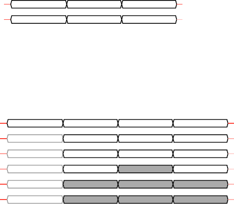
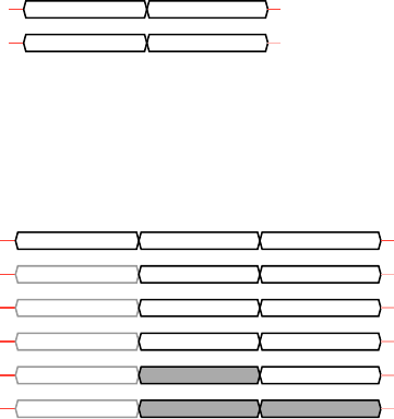
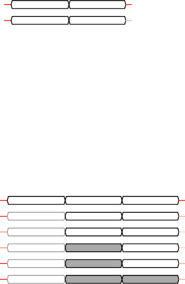
pen at the same time as a falling edge of the original clock. Figure2.1 shows two clock periods
of the system clock and an inverted clock derived from it, and how they are out of phase due
to clock inversion.
period period
also
a period
also
a period
Inverted 4 MiHz
CLK 4 MiHz
Figure2.1: Example clock periods
PHI 1 MiHz
CLK 4 MiHz
T1 T1 T2 T2 T3 T3 T4 T4
T1R T1F T2R T2F T3R T3F T4R T4F
Figure2.2: Clock edges in a machine cycle
14
Part II
Sharp SM83 CPU core
15

Chapter 3
Introduction
The CPU core in the Game Boy SoC is a custom Sharp design that hasn’t publicly been given
a name by either Sharp or Nintendo. However, using old Sharp datasheets and databooks as
evidence, the core has been identified to be a Sharp SM83 CPU core, or at least something
that is 100% compatible with it. SM83 is a custom CPU core used in some custom Application
Specific Integrated Chips (ASICs) manufactured by Sharp in the 1980s and 1990s.
Warning
Some sources claim Game Boy uses a “modified” Zilog Z80 or Intel 8080 CPU core.
While the SM83 resembles both and has many identical instructions, it can’t execute all
Z80/8080 programs, and finer details such as timing of instructions often differ.
SM83 is an 8-bit CPU core with a 16-bit address bus. The Instruction Set Architecture (ISA) is
based on both Z80 and 8080, and is close enough to Z80 that programmers familiar with Z80
assembly can quickly become productive with SM83 as well. Some Z80 programs may also work
directly on SM83, assuming only opcodes supported by both are used and the program is not
sensitive to timing differences.
🧩 Speculation
Sharp most likely designed SM83 to closely resemble Z80, so it would be easy for pro-
grammers already familiar with the widely popular Z80 to write programs for it. However,
SM83 is not a “modified Z80” because the internal implementation is completely differ-
ent. At the time Sharp also manufactured real Z80 chips such as LH0080 under a license
from Zilog, so they were familiar with Z80 internals but did not directly copy the actual
implementation of the CPU core. If you compare photos of a decapped Z80 chip and a
GB SoC, you will see two very different-looking CPU cores.
3.1 History
The first known mention of the SM83 CPU core is in Sharp Microcomputers Data Book (1990),
where it is listed as the CPU core used in the SM8320 8-bit microcomputer chip, intended for
inverter air conditioners [1]. The data book describes some details of the CPU core, such as a
high-level overview of the supported instructions, but precise details such as full opcode tables
are not included. Another CPU core called SM82 is also mentioned, but based on the details it’s
clearly a completely different one.
The SM83 CPU core later appeared in Sharp Microcomputer Data Book (1996), where it is listed
as the CPU core in the SM8311/SM8313/SM8314/SM8315 8-bit microcomputer chips, meant for
home appliances [2]. This data book describes the CPU core in much more detailed manner,
and other than some mistakes in the descriptions, the details seem to match what is known
about the GB SoC CPU core from other sources.
16

Chapter 4
Simple model
Figure4.3: Simple model of the SM83 CPU core
Figure4.3 shows a simplified model of the SM83 CPU core. The core interacts with the rest of
the SoC using interrupt signals, an 8-bit bidirectional data bus, and a 16-bit address bus con-
trolled by the CPU core.
The main subsystems of the CPU core are as follows:
Control unit The control unit decodes the executed instructions and generates control sig-
nals for the rest of the CPU core. It is also responsible for checking and dispatch-
ing interrupts.
Register file The register file holds most of the state of the CPU inside registers. It contains
the 16-bit Program Counter (PC), the 16-bit Stack Pointer (SP), the 8-bit Accu-
mulator (A), the Flags register (F), general-purpose register pairs consisting of
two 8-bit halves such as BC, DE, HL, and the special-purpose 8-bit registers In-
struction Register (IR) and Interrupt Enable (IE).
ALU An 8-bit Arithmetic Logic Unit (ALU) has two 8-bit input ports and is capable of
performing various calculations. The ALU outputs its result either to the regis-
ter file or the CPU data bus.
IDU A dedicated 16-bit Increment/Decrement Unit (IDU) is capable of performing
only simple increment/decrement operations on the 16-bit address bus value,
but they can be performed independently of the ALU, improving maximum per-
formance of the CPU core. The IDU always outputs its result back to the register
file, where it can be written to a register pair or a 16-bit register.
17

Chapter 5
CPU core timing
5.1 Fetch/execute overlap
Sharp SM83 uses a microprocessor design technique known as fetch/execute overlap to improve
CPU performance by doing opcode fetches in parallel with instruction execution whenever pos-
sible. Since the CPU can only perform one memory access per M-cycle, it is worth it to try to do
memory operations as soon as possible. Also, when doing a memory read, the CPU cannot use
the data during the same M-cycle so the true minimum effective duration of instructions is 2
machine cycles, not 1 machine cycle.
Every instruction needs one machine cycle for the fetch stage, and at least one machine cycle
for the decode/execute stage. However, the fetch stage of an instruction always overlaps with
the last machine cycle of the execute stage of the previous instruction. The overlapping execute
stage cycle may still do some work (e.g. ALU operation and/or register writeback) but memory
access is reserved for the fetch stage of the next instruction.
Since all instructions effectively last one machine cycle longer, fetch/execute overlap is usually
ignored in documentation intended for programmers. It is much easier to think of a program
as a sequence of non-overlapping instructions and consider only the execute stages when cal-
culating instruction durations. However, when emulating a SM83 CPU core, understanding and
emulating the overlap can be useful.
Warning
Sharp SM831x is a family of single-chip SoCs from Sharp that use the SM83 CPU core,
and their datasheet [3] includes a description of fetch/execute overlap. However, the de-
scription is not completely correct and can in fact be misleading.
For example, the timing diagram includes an instruction that does not involve opcode
fetch at all, and memory operations for two instructions are shown to happen at the
same time, which is not possible.
Fetch/execute overlap timing example
Let’s assume the CPU is executing a program that starts from the address 0x1000 and contains
the following instructions:
0x1000 INC A
0x1001 LDH (n), A
0x1003 RST 0x08
0x0008 NOP
The following timing diagram shows all memory operations done by the CPU, and the fetch
and execute stages of each instruction:
18

After NOP
NOP
RST 0x08
LDH (n), A
INC A
Before INC A
Mem addr
Mem R/W
PHI 1 MiHz
CLK 4 MiHz
M1: fetch
M1: fetch M2: execute
M1: fetch M2-5: execute
M1: fetch M2-4: execute
M1: fetch M2: execute
execute
0x1000 0x1001 0x1002 0xFF00+n 0x1003 SP-1 SP-2 0x0008 0x0009
R: opcode R: opcode R: n W: A R: opcode W: msb(PC) W: lsb(PC) R: opcode R: opcode
Figure5.4: Fetch/execute overlap example
19
Chapter 6
Sharp SM83 instruction set
6.1 Overview
CB opcode prefix
Undefined opcodes
20

6.2 8-bit load instructions
LD r, r’: Load register (register)
Load to the 8-bit register r, data from the 8-bit register r'.
Opcode 0b01xxxyyy/various Duration 1 machine cycle
Length 1 byte: opcode Flags -
Simple timing and pseudocode
Mem R/W
M-cycle
opcode
M1
opcode = read_memory(addr=PC); PC = PC + 1
if opcode == 0x41: # example: LD B, C
B = C
Detailed timing and pseudocode
Misc op
ALU op
IDU op
Data bus
Addr bus
M-cycle
Previous
Previous r ← r'
Previous PC ← PC + 1
IR ← mem IR ← mem
Previous PC
M1 M2/M1
# M2/M1
if IR == 0x41: # example: LD B, C
IR, intr = fetch_cycle(addr=PC); PC = PC + 1; B = C
21

LD r, n: Load register (immediate)
Load to the 8-bit register r, the immediate data n.
Opcode 0b00xxx110/various Duration 2 machine cycles
Length 2 bytes: opcode + n Flags -
Simple timing and pseudocode
Mem R/W
M-cycle
opcode R: n
M1 M2
opcode = read_memory(addr=PC); PC = PC + 1
if opcode == 0x06: # example: LD B, n
B = read_memory(addr=PC); PC = PC + 1
Detailed timing and pseudocode
Misc op
ALU op
IDU op
Data bus
Addr bus
M-cycle
Previous
Previous r ← Z
Previous PC ← PC + 1 PC ← PC + 1
IR ← mem Z ← mem IR ← mem
Previous PC PC
M1 M2 M3/M1
# M2
if IR == 0x06: # example: LD B, n
Z = read_memory(addr=PC); PC = PC + 1
# M3/M1
IR, intr = fetch_cycle(addr=PC); PC = PC + 1; B = Z
22

LD r, (HL): Load register (indirect HL)
Load to the 8-bit register r, data from the absolute address specified by the 16-bit register HL.
Opcode 0b01xxx110/various Duration 2 machine cycles
Length 1 byte: opcode Flags -
Simple timing and pseudocode
Mem R/W
M-cycle
opcode R: data
M1 M2
opcode = read_memory(addr=PC); PC = PC + 1
if opcode == 0x46: # example: LD B, (HL)
B = read_memory(addr=HL)
Detailed timing and pseudocode
Misc op
ALU op
IDU op
Data bus
Addr bus
M-cycle
Previous
Previous r ← Z
Previous PC ← PC + 1
IR ← mem Z ← mem IR ← mem
Previous HL PC
M1 M2 M3/M1
# M2
if IR == 0x46: # example: LD B, (HL)
Z = read_memory(addr=HL)
# M3/M1
IR, intr = fetch_cycle(addr=PC); PC = PC + 1; B = Z
23

LD (HL), r: Load from register (indirect HL)
Load to the absolute address specified by the 16-bit register HL, data from the 8-bit register r.
Opcode 0b01110xxx/various Duration 2 machine cycles
Length 1 byte: opcode Flags -
Simple timing and pseudocode
Mem R/W
M-cycle
opcode W: data
M1 M2
opcode = read_memory(addr=PC); PC = PC + 1
if opcode == 0x70: # example: LD (HL), B
write_memory(addr=HL, data=B)
Detailed timing and pseudocode
Misc op
ALU op
IDU op
Data bus
Addr bus
M-cycle
Previous
Previous
Previous PC ← PC + 1
IR ← mem mem ← r IR ← mem
Previous HL PC
M1 M2 M3/M1
# M2
if IR == 0x70: # example: LD (HL), B
write_memory(addr=HL, data=B)
# M3/M1
IR, intr = fetch_cycle(addr=PC); PC = PC + 1
24
LD (HL), n: Load from immediate data (indirect HL)
Load to the absolute address specified by the 16-bit register HL, the immediate data n.
Opcode 0b00110110/0x36 Duration 3 machine cycles
Length 2 bytes: opcode + n Flags -
Simple timing and pseudocode
Mem R/W
M-cycle
opcode R: n W: n
M1 M2 M3
opcode = read_memory(addr=PC); PC = PC + 1
if opcode == 0x36:
n = read_memory(addr=PC); PC = PC + 1
write_memory(addr=HL, data=n)
Detailed timing and pseudocode
Misc op
ALU op
IDU op
Data bus
Addr bus
M-cycle
Previous
Previous
Previous PC ← PC + 1 PC ← PC + 1
IR ← mem Z ← mem mem ← Z IR ← mem
Previous PC HL PC
M1 M2 M3 M4/M1
# M2
if IR == 0x36:
Z = read_memory(addr=PC); PC = PC + 1
# M3
write_memory(addr=HL, data=Z)
# M4/M1
IR, intr = fetch_cycle(addr=PC); PC = PC + 1
25

LD A, (BC): Load accumulator (indirect BC)
Load to the 8-bit A register, data from the absolute address specified by the 16-bit register BC.
Opcode 0b00001010/0x0A Duration 2 machine cycles
Length 1 byte: opcode Flags -
Simple timing and pseudocode
Mem R/W
M-cycle
opcode R: data
M1 M2
opcode = read_memory(addr=PC); PC = PC + 1
if opcode == 0x0A:
A = read_memory(addr=BC)
Detailed timing and pseudocode
Misc op
ALU op
IDU op
Data bus
Addr bus
M-cycle
Previous
Previous A ← Z
Previous PC ← PC + 1
IR ← mem Z ← mem IR ← mem
Previous BC PC
M1 M2 M3/M1
# M2
if IR == 0x0A:
Z = read_memory(addr=BC)
# M3/M1
IR, intr = fetch_cycle(addr=PC); PC = PC + 1; A = Z
26

LD A, (DE): Load accumulator (indirect DE)
Load to the 8-bit A register, data from the absolute address specified by the 16-bit register DE.
Opcode 0b00011010/0x1A Duration 2 machine cycles
Length 1 byte: opcode Flags -
Simple timing and pseudocode
Mem R/W
M-cycle
opcode R: data
M1 M2
opcode = read_memory(addr=PC); PC = PC + 1
if opcode == 0x1A:
A = read_memory(addr=DE)
Detailed timing and pseudocode
Misc op
ALU op
IDU op
Data bus
Addr bus
M-cycle
Previous
Previous A ← Z
Previous PC ← PC + 1
IR ← mem Z ← mem IR ← mem
Previous DE PC
M1 M2 M3/M1
# M2
if IR == 0x1A:
Z = read_memory(addr=DE)
# M3/M1
IR, intr = fetch_cycle(addr=PC); PC = PC + 1; A = Z
27

LD (BC), A: Load from accumulator (indirect BC)
Load to the absolute address specified by the 16-bit register BC, data from the 8-bit A register.
Opcode 0b00000010/0x02 Duration 2 machine cycles
Length 1 byte: opcode Flags -
Simple timing and pseudocode
Mem R/W
M-cycle
opcode W: data
M1 M2
opcode = read_memory(addr=PC); PC = PC + 1
if opcode == 0x02:
write_memory(addr=BC, data=A)
Detailed timing and pseudocode
Misc op
ALU op
IDU op
Data bus
Addr bus
M-cycle
Previous
Previous
Previous PC ← PC + 1
IR ← mem mem ← A IR ← mem
Previous BC PC
M1 M2 M3/M1
# M2
if IR == 0x02:
write_memory(addr=BC, data=A)
# M3/M1
IR, intr = fetch_cycle(addr=PC); PC = PC + 1
28

LD (DE), A: Load from accumulator (indirect DE)
Load to the absolute address specified by the 16-bit register DE, data from the 8-bit A register.
Opcode 0b00010010/0x12 Duration 2 machine cycles
Length 1 byte: opcode Flags -
Simple timing and pseudocode
Mem R/W
M-cycle
opcode W: data
M1 M2
opcode = read_memory(addr=PC); PC = PC + 1
if opcode == 0x12:
write_memory(addr=DE, data=A)
Detailed timing and pseudocode
Misc op
ALU op
IDU op
Data bus
Addr bus
M-cycle
Previous
Previous
Previous PC ← PC + 1
IR ← mem mem ← A IR ← mem
Previous DE PC
M1 M2 M3/M1
# M2
if IR == 0x12:
write_memory(addr=DE, data=A)
# M3/M1
IR, intr = fetch_cycle(addr=PC); PC = PC + 1
29

LD A, (nn): Load accumulator (direct)
Load to the 8-bit A register, data from the absolute address specified by the 16-bit operand nn.
Opcode 0b11111010/0xFA Duration 4 machine cycles
Length 3 bytes: opcode + LSB(nn) + MSB(nn) Flags -
Simple timing and pseudocode
Mem R/W
M-cycle
opcode R: lsb nn R: msb nn R: data
M1 M2 M3 M4
opcode = read_memory(addr=PC); PC = PC + 1
if opcode == 0xFA:
nn_lsb = read_memory(addr=PC); PC = PC + 1
nn_msb = read_memory(addr=PC); PC = PC + 1
nn = unsigned_16(lsb=nn_lsb, msb=nn_msb)
A = read_memory(addr=nn)
Detailed timing and pseudocode
Misc op
ALU op
IDU op
Data bus
Addr bus
M-cycle
Previous
Previous A ← Z
Previous PC ← PC + 1 PC ← PC + 1 PC ← PC + 1
IR ← mem Z ← mem W ← mem Z ← mem IR ← mem
Previous PC PC WZ PC
M1 M2 M3 M4 M5/M1
# M2
if IR == 0xFA:
Z = read_memory(addr=PC); PC = PC + 1
# M3
W = read_memory(addr=PC); PC = PC + 1
# M4
Z = read_memory(addr=WZ)
# M5/M1
IR, intr = fetch_cycle(addr=PC); PC = PC + 1; A = Z
30

LD (nn), A: Load from accumulator (direct)
Load to the absolute address specified by the 16-bit operand nn, data from the 8-bit A register.
Opcode 0b11101010/0xEA Duration 4 machine cycles
Length 3 bytes: opcode + LSB(nn) + MSB(nn) Flags -
Simple timing and pseudocode
Mem R/W
M-cycle
opcode R: lsb nn R: msb nn W: data
M1 M2 M3 M4
opcode = read_memory(addr=PC); PC = PC + 1
if opcode == 0xEA:
nn_lsb = read_memory(addr=PC); PC = PC + 1
nn_msb = read_memory(addr=PC); PC = PC + 1
nn = unsigned_16(lsb=nn_lsb, msb=nn_msb)
write_memory(addr=nn, data=A)
Detailed timing and pseudocode
Misc op
ALU op
IDU op
Data bus
Addr bus
M-cycle
Previous
Previous
Previous PC ← PC + 1 PC ← PC + 1 PC ← PC + 1
IR ← mem Z ← mem W ← mem mem ← A IR ← mem
Previous PC PC WZ PC
M1 M2 M3 M4 M5/M1
# M2
if IR == 0xEA:
Z = read_memory(addr=PC); PC = PC + 1
# M3
W = read_memory(addr=PC); PC = PC + 1
# M4
write_memory(addr=WZ, data=A)
# M5/M1
IR, intr = fetch_cycle(addr=PC); PC = PC + 1
31

LDH A, (C): Load accumulator (indirect 0xFF00+C)
Load to the 8-bit A register, data from the address specified by the 8-bit C register. The full 16-bit
absolute address is obtained by setting the most significant byte to 0xFF and the least signifi-
cant byte to the value of C, so the possible range is 0xFF00-0xFFFF.
Opcode 0b11110010/0xF2 Duration 2 machine cycles
Length 1 byte: opcode Flags -
Simple timing and pseudocode
Mem R/W
M-cycle
opcode R: data
M1 M2
opcode = read_memory(addr=PC); PC = PC + 1
if opcode == 0xF2:
A = read_memory(addr=unsigned_16(lsb=C, msb=0xFF))
Detailed timing and pseudocode
Misc op
ALU op
IDU op
Data bus
Addr bus
M-cycle
Previous
Previous A ← Z
Previous PC ← PC + 1
IR ← mem Z ← mem IR ← mem
Previous 0xFF00+C PC
M1 M2 M3/M1
# M2
if IR == 0xF2:
Z = read_memory(addr=unsigned_16(lsb=C, msb=0xFF))
# M3/M1
IR, intr = fetch_cycle(addr=PC); PC = PC + 1; A = Z
32

LDH (C), A: Load from accumulator (indirect 0xFF00+C)
Load to the address specified by the 8-bit C register, data from the 8-bit A register. The full 16-bit
absolute address is obtained by setting the most significant byte to 0xFF and the least signifi-
cant byte to the value of C, so the possible range is 0xFF00-0xFFFF.
Opcode 0b11100010/0xE2 Duration 2 machine cycles
Length 1 byte: opcode Flags -
Simple timing and pseudocode
Mem R/W
M-cycle
opcode W: data
M1 M2
opcode = read_memory(addr=PC); PC = PC + 1
if opcode == 0xE2:
write_memory(addr=unsigned_16(lsb=C, data=msb=0xFF), data=A)
Detailed timing and pseudocode
Misc op
ALU op
IDU op
Data bus
Addr bus
M-cycle
Previous
Previous
Previous PC ← PC + 1
IR ← mem mem ← A IR ← mem
Previous 0xFF00+C PC
M1 M2 M3/M1
# M2
if IR == 0xE2:
write_memory(addr=unsigned_16(lsb=C, data=msb=0xFF), data=A)
# M3/M1
IR, intr = fetch_cycle(addr=PC); PC = PC + 1
33

LDH A, (n): Load accumulator (direct 0xFF00+n)
Load to the 8-bit A register, data from the address specified by the 8-bit immediate data n. The
full 16-bit absolute address is obtained by setting the most significant byte to 0xFF and the
least significant byte to the value of n, so the possible range is 0xFF00-0xFFFF.
Opcode 0b11110000/0xF0 Duration 3 machine cycles
Length 2 bytes: opcode + n Flags -
Simple timing and pseudocode
Mem R/W
M-cycle
opcode R: n R: data
M1 M2 M3
opcode = read_memory(addr=PC); PC = PC + 1
if opcode == 0xF0:
n = read_memory(addr=PC); PC = PC + 1
A = read_memory(addr=unsigned_16(lsb=n, msb=0xFF))
Detailed timing and pseudocode
Misc op
ALU op
IDU op
Data bus
Addr bus
M-cycle
Previous
Previous A ← Z
Previous PC ← PC + 1 PC ← PC + 1
IR ← mem Z ← mem Z ← mem IR ← mem
Previous PC 0xFF00+Z PC
M1 M2 M3 M4/M1
# M2
if IR == 0xF0:
Z = read_memory(addr=PC); PC = PC + 1
# M3
Z = read_memory(addr=unsigned_16(lsb=Z, msb=0xFF))
# M4/M1
IR, intr = fetch_cycle(addr=PC); PC = PC + 1; A = Z
34

LDH (n), A: Load from accumulator (direct 0xFF00+n)
Load to the address specified by the 8-bit immediate data n, data from the 8-bit A register. The
full 16-bit absolute address is obtained by setting the most significant byte to 0xFF and the
least significant byte to the value of n, so the possible range is 0xFF00-0xFFFF.
Opcode 0b11100000/0xE0 Duration 3 machine cycles
Length 2 bytes: opcode + n Flags -
Simple timing and pseudocode
Mem R/W
M-cycle
opcode R: n W: data
M1 M2 M3
opcode = read_memory(addr=PC); PC = PC + 1
if opcode == 0xE0:
n = read_memory(addr=PC); PC = PC + 1
write_memory(addr=unsigned_16(lsb=n, msb=0xFF), data=A)
Detailed timing and pseudocode
Misc op
ALU op
IDU op
Data bus
Addr bus
M-cycle
Previous
Previous
Previous PC ← PC + 1 PC ← PC + 1
IR ← mem Z ← mem mem ← A IR ← mem
Previous PC 0xFF00+Z PC
M1 M2 M3 M4/M1
# M2
if IR == 0xE0:
Z = read_memory(addr=PC); PC = PC + 1
# M3
write_memory(addr=unsigned_16(lsb=Z, msb=0xFF), data=A)
# M4/M1
IR, intr = fetch_cycle(addr=PC); PC = PC + 1
35

LD A, (HL-): Load accumulator (indirect HL, decrement)
Load to the 8-bit A register, data from the absolute address specified by the 16-bit register HL.
The value of HL is decremented after the memory read.
Opcode 0b00111010/0x3A Duration 2 machine cycles
Length 1 byte: opcode Flags -
Simple timing and pseudocode
Mem R/W
M-cycle
opcode R: data
M1 M2
opcode = read_memory(addr=PC); PC = PC + 1
if opcode == 0x3A:
A = read_memory(addr=HL); HL = HL - 1
Detailed timing and pseudocode
Misc op
ALU op
IDU op
Data bus
Addr bus
M-cycle
Previous
Previous A ← Z
Previous HL ← HL - 1 PC ← PC + 1
IR ← mem Z ← mem IR ← mem
Previous HL PC
M1 M2 M3/M1
# M2
if IR == 0x3A:
Z = read_memory(addr=HL); HL = HL - 1
# M3/M1
IR, intr = fetch_cycle(addr=PC); PC = PC + 1; A = Z
36

LD (HL-), A: Load from accumulator (indirect HL, decrement)
Load to the absolute address specified by the 16-bit register HL, data from the 8-bit A register.
The value of HL is decremented after the memory write.
Opcode 0b00110010/0x32 Duration 2 machine cycles
Length 1 byte: opcode Flags -
Simple timing and pseudocode
Mem R/W
M-cycle
opcode W: data
M1 M2
opcode = read_memory(addr=PC); PC = PC + 1
if opcode == 0x32:
write_memory(addr=HL, data=A); HL = HL - 1
Detailed timing and pseudocode
Misc op
ALU op
IDU op
Data bus
Addr bus
M-cycle
Previous
Previous
Previous HL ← HL - 1 PC ← PC + 1
IR ← mem mem ← A IR ← mem
Previous HL PC
M1 M2 M3/M1
# M2
if IR == 0x32:
write_memory(addr=HL, data=A); HL = HL - 1
# M3/M1
IR, intr = fetch_cycle(addr=PC); PC = PC + 1
37
LD A, (HL+): Load accumulator (indirect HL, increment)
Load to the 8-bit A register, data from the absolute address specified by the 16-bit register HL.
The value of HL is incremented after the memory read.
Opcode 0b00101010/0x2A Duration 2 machine cycles
Length 1 byte: opcode Flags -
Simple timing and pseudocode
Mem R/W
M-cycle
opcode R: data
M1 M2
opcode = read_memory(addr=PC); PC = PC + 1
if opcode == 0x2A:
A = read_memory(addr=HL); HL = HL + 1
Detailed timing and pseudocode
Misc op
ALU op
IDU op
Data bus
Addr bus
M-cycle
Previous
Previous A ← Z
Previous HL ← HL + 1 PC ← PC + 1
IR ← mem Z ← mem IR ← mem
Previous HL PC
M1 M2 M3/M1
# M2
if IR == 0x2A:
Z = read_memory(addr=HL); HL = HL + 1
# M3/M1
IR, intr = fetch_cycle(addr=PC); PC = PC + 1; A = Z
38

LD (HL+), A: Load from accumulator (indirect HL, increment)
Load to the absolute address specified by the 16-bit register HL, data from the 8-bit A register.
The value of HL is decremented after the memory write.
Opcode 0b00100010/0x22 Duration 2 machine cycles
Length 1 byte: opcode Flags -
Simple timing and pseudocode
Mem R/W
M-cycle
opcode W: data
M1 M2
opcode = read_memory(addr=PC); PC = PC + 1
if opcode == 0x22:
write_memory(addr=HL, data=A); HL = HL + 1
Detailed timing and pseudocode
Misc op
ALU op
IDU op
Data bus
Addr bus
M-cycle
Previous
Previous
Previous HL ← HL + 1 PC ← PC + 1
IR ← mem mem ← A IR ← mem
Previous HL PC
M1 M2 M3/M1
# M2
if IR == 0x22:
write_memory(addr=HL, data=A); HL = HL + 1
# M3/M1
IR, intr = fetch_cycle(addr=PC); PC = PC + 1
39

6.3 16-bit load instructions
LD rr, nn: Load 16-bit register / register pair
Load to the 16-bit register rr, the immediate 16-bit data nn.
Opcode 0b00xx0001/various Duration 3 machine cycles
Length 3 bytes: opcode + LSB(nn) + MSB(nn) Flags -
Simple timing and pseudocode
Mem R/W
M-cycle
opcode R: lsb nn R: msb nn
M1 M2 M3
opcode = read_memory(addr=PC); PC = PC + 1
if opcode == 0x01: # example: LD BC, nn
nn_lsb = read_memory(addr=PC); PC = PC + 1
nn_msb = read_memory(addr=PC); PC = PC + 1
nn = unsigned_16(lsb=nn_lsb, msb=nn_msb)
BC = nn
Detailed timing and pseudocode
Misc op
ALU op
IDU op
Data bus
Addr bus
M-cycle
Previous rr ← WZ
Previous
Previous PC ← PC + 1 PC ← PC + 1 PC ← PC + 1
IR ← mem Z ← mem W ← mem IR ← mem
Previous PC PC PC
M1 M2 M3 M4/M1
# M2
if IR == 0x01: # example: LD BC, nn
Z = read_memory(addr=PC); PC = PC + 1
# M3
W = read_memory(addr=PC); PC = PC + 1
# M4/M1
IR, intr = fetch_cycle(addr=PC); PC = PC + 1; BC = WZ
40

LD (nn), SP: Load from stack pointer (direct)
Load to the absolute address specified by the 16-bit operand nn, data from the 16-bit SP reg-
ister.
Opcode 0b00001000/0x08 Duration 5 machine cycles
Length 3 bytes: opcode + LSB(nn) + MSB(nn) Flags -
Simple timing and pseudocode
Mem R/W
M-cycle
opcode R: Z R: W W: SPH W: SPL
M1 M2 M3 M4 M5
opcode = read_memory(addr=PC); PC = PC + 1
if opcode == 0x08:
nn_lsb = read_memory(addr=PC); PC = PC + 1
nn_msb = read_memory(addr=PC); PC = PC + 1
nn = unsigned_16(lsb=nn_lsb, msb=nn_msb)
write_memory(addr=nn, data=lsb(SP)); nn = nn + 1
write_memory(addr=nn, data=msb(SP))
Detailed timing and pseudocode
Misc op
ALU op
IDU op
Data bus
Addr bus
M-cycle
Previous
Previous
Previous PC ← PC + 1 PC ← PC + 1 WZ ← WZ + 1 PC ← PC + 1
IR ← mem Z ← mem W ← mem mem ← SPL mem ← SPH IR ← mem
Previous PC PC WZ WZ PC
M1 M2 M3 M4 M5 M6/M1
# M2
if IR == 0x08:
Z = read_memory(addr=PC); PC = PC + 1
# M3
W = read_memory(addr=PC); PC = PC + 1
# M4
write_memory(addr=WZ, data=lsb(SP)); WZ = WZ + 1
# M5
write_memory(addr=WZ, data=msb(SP))
# M6/M1
IR, intr = fetch_cycle(addr=PC); PC = PC + 1
41

LD SP, HL: Load stack pointer from HL
Load to the 16-bit SP register, data from the 16-bit HL register.
Opcode 0b11111001/0xF9 Duration 2 machine cycles
Length 1 byte: opcode Flags -
Simple timing and pseudocode
Mem R/W
M-cycle
opcode
M1 M2
opcode = read_memory(addr=PC); PC = PC + 1
if opcode == 0xF9:
SP = HL
Detailed timing and pseudocode
Misc op
ALU op
IDU op
Data bus
Addr bus
M-cycle
Previous
Previous
Previous SP ← HL PC ← PC + 1
IR ← mem IR ← mem
Previous HL PC
M1 M2 M3/M1
# M2
if IR == 0xF9:
SP = HL
# M3/M1
IR, intr = fetch_cycle(addr=PC); PC = PC + 1
42

PUSH rr: Push to stack
Push to the stack memory, data from the 16-bit register rr.
Opcode 0b11xx0101/various Duration 4 machine cycles
Length 1 byte: opcode Flags -
Simple timing and pseudocode
Mem R/W
M-cycle
opcode W: msb rr W: lsb rr
M1 M2 M3 M4
opcode = read_memory(addr=PC); PC = PC + 1
if opcode == 0xC5: # example: PUSH BC
SP = SP - 1
write_memory(addr=SP, data=msb(BC)); SP = SP - 1
write_memory(addr=SP, data=lsb(BC))
Detailed timing and pseudocode
Misc op
ALU op
IDU op
Data bus
Addr bus
M-cycle
Previous
Previous
Previous SP ← SP - 1 SP ← SP - 1 SP ← SP PC ← PC + 1
IR ← mem mem ← msb rr mem ← lsb rr IR ← mem
Previous SP SP SP PC
M1 M2 M3 M4 M5/M1
# M2
if IR == 0xC5: # example: PUSH BC
SP = SP - 1
# M3
write_memory(addr=SP, data=msb(BC)); SP = SP - 1
# M4
write_memory(addr=SP, data=lsb(BC))
# M5/M1
IR, intr = fetch_cycle(addr=PC); PC = PC + 1
43

POP rr: Pop from stack
Pops to the 16-bit register rr, data from the stack memory.
This instruction does not do calculations that affect flags, but POP AF completely replaces the
F register value, so all flags are changed based on the 8-bit data that is read from memory.
Opcode 0b11xx0001/various Duration 3 machine cycles
Length 1 byte: opcode Flags See the instruction description
Simple timing and pseudocode
Mem R/W
M-cycle
opcode R: lsb rr R: msb rr
M1 M2 M3
opcode = read_memory(addr=PC); PC = PC + 1
if opcode == 0xC1: # example: POP BC
lsb = read_memory(addr=SP); SP = SP + 1
msb = read_memory(addr=SP); SP = SP + 1
BC = unsigned_16(lsb=lsb, msb=msb)
Detailed timing and pseudocode
Misc op
ALU op
IDU op
Data bus
Addr bus
M-cycle
Previous rr ← WZ
Previous
Previous SP ← SP + 1 SP ← SP + 1 PC ← PC + 1
IR ← mem Z ← mem W ← mem IR ← mem
Previous SP SP PC
M1 M2 M3 M4/M1
# M2
if IR == 0xC1: # example: POP BC
Z = read_memory(addr=SP); SP = SP + 1
# M3
W = read_memory(addr=SP); SP = SP + 1
# M4/M1
IR, intr = fetch_cycle(addr=PC); PC = PC + 1; BC = WZ
44

LD HL, SP+e: Load HL from adjusted stack pointer
Load to the HL register, 16-bit data calculated by adding the signed 8-bit operand e to the 16-
bit value of the SP register.
Opcode 0b11111000/0xF8 Duration 3 machine cycles
Length 2 bytes: opcode + e Flags
Z = 0, N = 0, H = ⭐, C = ⭐
Simple timing and pseudocode
Mem R/W
M-cycle
opcode R: e
M1 M2 M3
opcode = read_memory(addr=PC); PC = PC + 1
if opcode == 0xF8:
e = signed_8(read_memory(addr=PC)); PC = PC + 1
result, carry_per_bit = SP + e
HL = result
flags.Z = 0
flags.N = 0
flags.H = 1 if carry_per_bit[3] else 0
flags.C = 1 if carry_per_bit[7] else 0
Detailed timing and pseudocode
Misc op
ALU op
IDU op
Data bus
Addr bus
M-cycle
Previous
Previous L ← SPL + Z H ← SPH +
c
adj
Previous PC ← PC + 1 PC ← PC + 1
IR ← mem Z ← mem IR ← mem
Previous PC
0x0000
PC
M1 M2 M3 M4/M1
# M2
if IR == 0xF8:
Z = read_memory(addr=PC); PC = PC + 1
# M3
result, carry_per_bit = lsb(SP) + Z
L = result
flags.Z = 0
flags.N = 0
flags.H = 1 if carry_per_bit[3] else 0
flags.C = 1 if carry_per_bit[7] else 0
Z_sign = bit(7, Z)
# M4/M1
adj = 0xFF if Z_sign else 0x00
result = msb(SP) + adj + flags.C
H = result
IR, intr = fetch_cycle(addr=PC); PC = PC + 1
45

6.4 8-bit arithmetic and logical instructions
ADD r: Add (register)
Adds to the 8-bit A register, the 8-bit register r, and stores the result back into the A register.
Opcode 0b10000xxx/various Duration 1 machine cycle
Length 1 byte: opcode Flags
Z = ⭐, N = 0, H = ⭐, C = ⭐
Simple timing and pseudocode
Mem R/W
M-cycle
opcode
M1
opcode = read_memory(addr=PC); PC = PC + 1
if opcode == 0x80: # example: ADD B
result, carry_per_bit = A + B
A = result
flags.Z = 1 if result == 0 else 0
flags.N = 0
flags.H = 1 if carry_per_bit[3] else 0
flags.C = 1 if carry_per_bit[7] else 0
Detailed timing and pseudocode
Misc op
ALU op
IDU op
Data bus
Addr bus
M-cycle
Previous
Previous A ← A + r
Previous PC ← PC + 1
IR ← mem IR ← mem
Previous PC
M1 M2/M1
# M2/M1
if IR == 0x80: # example: ADD B
result, carry_per_bit = A + B
A = result
flags.Z = 1 if result == 0 else 0
flags.N = 0
flags.H = 1 if carry_per_bit[3] else 0
flags.C = 1 if carry_per_bit[7] else 0
IR, intr = fetch_cycle(addr=PC); PC = PC + 1
46
ADD (HL): Add (indirect HL)
Adds to the 8-bit A register, data from the absolute address specified by the 16-bit register HL,
and stores the result back into the A register.
Opcode 0b10000110/0x86 Duration 2 machine cycles
Length 1 byte: opcode Flags
Z = ⭐, N = 0, H = ⭐, C = ⭐
Simple timing and pseudocode
Mem R/W
M-cycle
opcode R: data
M1 M2
opcode = read_memory(addr=PC); PC = PC + 1
if opcode == 0x86:
data = read_memory(addr=HL)
result, carry_per_bit = A + data
A = result
flags.Z = 1 if result == 0 else 0
flags.N = 0
flags.H = 1 if carry_per_bit[3] else 0
flags.C = 1 if carry_per_bit[7] else 0
Detailed timing and pseudocode
Misc op
ALU op
IDU op
Data bus
Addr bus
M-cycle
Previous
Previous A ← A + Z
Previous PC ← PC + 1
IR ← mem Z ← mem IR ← mem
Previous HL PC
M1 M2 M3/M1
# M2
if IR == 0x86:
Z = read_memory(addr=HL)
# M3/M1
result, carry_per_bit = A + Z
A = result
flags.Z = 1 if result == 0 else 0
flags.N = 0
flags.H = 1 if carry_per_bit[3] else 0
flags.C = 1 if carry_per_bit[7] else 0
IR, intr = fetch_cycle(addr=PC); PC = PC + 1
47

ADD n: Add (immediate)
Adds to the 8-bit A register, the immediate data n, and stores the result back into the A register.
Opcode 0b11000110/0xC6 Duration 2 machine cycles
Length 2 bytes: opcode + n Flags
Z = ⭐, N = 0, H = ⭐, C = ⭐
Simple timing and pseudocode
Mem R/W
M-cycle
opcode R: n
M1 M2
opcode = read_memory(addr=PC); PC = PC + 1
if opcode == 0xC6:
n = read_memory(addr=PC); PC = PC + 1
result, carry_per_bit = A + n
A = result
flags.Z = 1 if result == 0 else 0
flags.N = 0
flags.H = 1 if carry_per_bit[3] else 0
flags.C = 1 if carry_per_bit[7] else 0
Detailed timing and pseudocode
Misc op
ALU op
IDU op
Data bus
Addr bus
M-cycle
Previous
Previous A ← A + Z
Previous PC ← PC + 1 PC ← PC + 1
IR ← mem Z ← mem IR ← mem
Previous PC PC
M1 M2 M3/M1
# M2
if IR == 0xC6:
Z = read_memory(addr=PC); PC = PC + 1
# M3/M1
result, carry_per_bit = A + Z
A = result
flags.Z = 1 if result == 0 else 0
flags.N = 0
flags.H = 1 if carry_per_bit[3] else 0
flags.C = 1 if carry_per_bit[7] else 0
IR, intr = fetch_cycle(addr=PC); PC = PC + 1
48

ADC r: Add with carry (register)
Adds to the 8-bit A register, the carry flag and the 8-bit register r, and stores the result back
into the A register.
Opcode 0b10001xxx/various Duration 1 machine cycle
Length 1 byte: opcode Flags
Z = ⭐, N = 0, H = ⭐, C = ⭐
Simple timing and pseudocode
Mem R/W
M-cycle
opcode
M1
opcode = read_memory(addr=PC); PC = PC + 1
if opcode == 0x88: # example: ADC B
result, carry_per_bit = A + B + flags.C
A = result
flags.Z = 1 if result == 0 else 0
flags.N = 0
flags.H = 1 if carry_per_bit[3] else 0
flags.C = 1 if carry_per_bit[7] else 0
Detailed timing and pseudocode
Misc op
ALU op
IDU op
Data bus
Addr bus
M-cycle
Previous
Previous A ← A +
c
r
Previous PC ← PC + 1
IR ← mem IR ← mem
Previous PC
M1 M2/M1
# M2/M1
if IR == 0x88: # example: ADC B
result, carry_per_bit = A + B + flags.C
A = result
flags.Z = 1 if result == 0 else 0
flags.N = 0
flags.H = 1 if carry_per_bit[3] else 0
flags.C = 1 if carry_per_bit[7] else 0
IR, intr = fetch_cycle(addr=PC); PC = PC + 1
49

ADC (HL): Add with carry (indirect HL)
Adds to the 8-bit A register, the carry flag and data from the absolute address specified by the
16-bit register HL, and stores the result back into the A register.
Opcode 0b10001110/0x8E Duration 2 machine cycles
Length 1 byte: opcode Flags
Z = ⭐, N = 0, H = ⭐, C = ⭐
Simple timing and pseudocode
Mem R/W
M-cycle
opcode R: data
M1 M2
opcode = read_memory(addr=PC); PC = PC + 1
if opcode == 0x8E:
data = read_memory(addr=HL)
result, carry_per_bit = A + data + flags.C
A = result
flags.Z = 1 if result == 0 else 0
flags.N = 0
flags.H = 1 if carry_per_bit[3] else 0
flags.C = 1 if carry_per_bit[7] else 0
Detailed timing and pseudocode
Misc op
ALU op
IDU op
Data bus
Addr bus
M-cycle
Previous
Previous A ← A +
c
Z
Previous PC ← PC + 1
IR ← mem Z ← mem IR ← mem
Previous HL PC
M1 M2 M3/M1
# M2
if IR == 0x8E:
Z = read_memory(addr=HL)
# M3/M1
result, carry_per_bit = A + Z + flags.C
A = result
flags.Z = 1 if result == 0 else 0
flags.N = 0
flags.H = 1 if carry_per_bit[3] else 0
flags.C = 1 if carry_per_bit[7] else 0
IR, intr = fetch_cycle(addr=PC); PC = PC + 1
50

ADC n: Add with carry (immediate)
Adds to the 8-bit A register, the carry flag and the immediate data n, and stores the result back
into the A register.
Opcode 0b11001110/0xCE Duration 2 machine cycles
Length 2 bytes: opcode + n Flags
Z = ⭐, N = 0, H = ⭐, C = ⭐
Simple timing and pseudocode
Mem R/W
M-cycle
opcode R: n
M1 M2
opcode = read_memory(addr=PC); PC = PC + 1
if opcode == 0xCE:
n = read_memory(addr=PC); PC = PC + 1
result, carry_per_bit = A + n + flags.C
A = result
flags.Z = 1 if result == 0 else 0
flags.N = 0
flags.H = 1 if carry_per_bit[3] else 0
flags.C = 1 if carry_per_bit[7] else 0
Detailed timing and pseudocode
Misc op
ALU op
IDU op
Data bus
Addr bus
M-cycle
Previous
Previous A ← A +
c
Z
Previous PC ← PC + 1 PC ← PC + 1
IR ← mem Z ← mem IR ← mem
Previous PC PC
M1 M2 M3/M1
# M2
if IR == 0xCE:
Z = read_memory(addr=PC); PC = PC + 1
# M3/M1
result, carry_per_bit = A + Z + flags.C
A = result
flags.Z = 1 if result == 0 else 0
flags.N = 0
flags.H = 1 if carry_per_bit[3] else 0
flags.C = 1 if carry_per_bit[7] else 0
IR, intr = fetch_cycle(addr=PC); PC = PC + 1
51

SUB r: Subtract (register)
Subtracts from the 8-bit A register, the 8-bit register r, and stores the result back into the A
register.
Opcode 0b10010xxx/various Duration 1 machine cycle
Length 1 byte: opcode Flags
Z = ⭐, N = 1, H = ⭐, C = ⭐
Simple timing and pseudocode
Mem R/W
M-cycle
opcode
M1
opcode = read_memory(addr=PC); PC = PC + 1
if opcode == 0x90: # example: SUB B
result, carry_per_bit = A - B
A = result
flags.Z = 1 if result == 0 else 0
flags.N = 1
flags.H = 1 if carry_per_bit[3] else 0
flags.C = 1 if carry_per_bit[7] else 0
Detailed timing and pseudocode
Misc op
ALU op
IDU op
Data bus
Addr bus
M-cycle
Previous
Previous A ← A - r
Previous PC ← PC + 1
IR ← mem IR ← mem
Previous PC
M1 M2/M1
# M2/M1
if IR == 0x90: # example: SUB B
result, carry_per_bit = A - B
A = result
flags.Z = 1 if result == 0 else 0
flags.N = 1
flags.H = 1 if carry_per_bit[3] else 0
flags.C = 1 if carry_per_bit[7] else 0
IR, intr = fetch_cycle(addr=PC); PC = PC + 1
52

SUB (HL): Subtract (indirect HL)
Subtracts from the 8-bit A register, data from the absolute address specified by the 16-bit reg-
ister HL, and stores the result back into the A register.
Opcode 0b10010110/0x96 Duration 2 machine cycles
Length 1 byte: opcode Flags
Z = ⭐, N = 1, H = ⭐, C = ⭐
Simple timing and pseudocode
Mem R/W
M-cycle
opcode R: data
M1 M2
opcode = read_memory(addr=PC); PC = PC + 1
if opcode == 0x96:
data = read_memory(addr=HL)
result, carry_per_bit = A - data
A = result
flags.Z = 1 if result == 0 else 0
flags.N = 1
flags.H = 1 if carry_per_bit[3] else 0
flags.C = 1 if carry_per_bit[7] else 0
Detailed timing and pseudocode
Misc op
ALU op
IDU op
Data bus
Addr bus
M-cycle
Previous
Previous A ← A - Z
Previous PC ← PC + 1
IR ← mem Z ← mem IR ← mem
Previous HL PC
M1 M2 M3/M1
# M2
if IR == 0x96:
Z = read_memory(addr=HL)
# M3/M1
result, carry_per_bit = A - Z
A = result
flags.Z = 1 if result == 0 else 0
flags.N = 1
flags.H = 1 if carry_per_bit[3] else 0
flags.C = 1 if carry_per_bit[7] else 0
IR, intr = fetch_cycle(addr=PC); PC = PC + 1
53

SUB n: Subtract (immediate)
Subtracts from the 8-bit A register, the immediate data n, and stores the result back into the A
register.
Opcode 0b11010110/0xD6 Duration 2 machine cycles
Length 2 bytes: opcode + n Flags
Z = ⭐, N = 1, H = ⭐, C = ⭐
Simple timing and pseudocode
Mem R/W
M-cycle
opcode R: n
M1 M2
opcode = read_memory(addr=PC); PC = PC + 1
if opcode == 0xD6:
n = read_memory(addr=PC); PC = PC + 1
result, carry_per_bit = A - n
A = result
flags.Z = 1 if result == 0 else 0
flags.N = 1
flags.H = 1 if carry_per_bit[3] else 0
flags.C = 1 if carry_per_bit[7] else 0
Detailed timing and pseudocode
Misc op
ALU op
IDU op
Data bus
Addr bus
M-cycle
Previous
Previous A ← A - Z
Previous PC ← PC + 1 PC ← PC + 1
IR ← mem Z ← mem IR ← mem
Previous PC PC
M1 M2 M3/M1
# M2
if IR == 0xD6:
Z = read_memory(addr=PC); PC = PC + 1
# M3/M1
result, carry_per_bit = A - Z
A = result
flags.Z = 1 if result == 0 else 0
flags.N = 1
flags.H = 1 if carry_per_bit[3] else 0
flags.C = 1 if carry_per_bit[7] else 0
IR, intr = fetch_cycle(addr=PC); PC = PC + 1
54

SBC r: Subtract with carry (register)
Subtracts from the 8-bit A register, the carry flag and the 8-bit register r, and stores the result
back into the A register.
Opcode 0b10011xxx/various Duration 1 machine cycle
Length 1 byte: opcode Flags
Z = ⭐, N = 1, H = ⭐, C = ⭐
Simple timing and pseudocode
Mem R/W
M-cycle
opcode
M1
opcode = read_memory(addr=PC); PC = PC + 1
if opcode == 0x98: # example: SBC B
result, carry_per_bit = A - B - flags.C
A = result
flags.Z = 1 if result == 0 else 0
flags.N = 1
flags.H = 1 if carry_per_bit[3] else 0
flags.C = 1 if carry_per_bit[7] else 0
Detailed timing and pseudocode
Misc op
ALU op
IDU op
Data bus
Addr bus
M-cycle
Previous
Previous A ← A -
c
r
Previous PC ← PC + 1
IR ← mem IR ← mem
Previous PC
M1 M2/M1
# M2/M1
if IR == 0x98: # example: SBC B
result, carry_per_bit = A - B - flags.C
A = result
flags.Z = 1 if result == 0 else 0
flags.N = 1
flags.H = 1 if carry_per_bit[3] else 0
flags.C = 1 if carry_per_bit[7] else 0
IR, intr = fetch_cycle(addr=PC); PC = PC + 1
55

SBC (HL): Subtract with carry (indirect HL)
Subtracts from the 8-bit A register, the carry flag and data from the absolute address specified
by the 16-bit register HL, and stores the result back into the A register.
Opcode 0b10011110/0x9E Duration 2 machine cycles
Length 1 byte: opcode Flags
Z = ⭐, N = 1, H = ⭐, C = ⭐
Simple timing and pseudocode
Mem R/W
M-cycle
opcode R: data
M1 M2
opcode = read_memory(addr=PC); PC = PC + 1
if opcode == 0x9E:
data = read_memory(addr=HL)
result, carry_per_bit = A - data - flags.C
A = result
flags.Z = 1 if result == 0 else 0
flags.N = 1
flags.H = 1 if carry_per_bit[3] else 0
flags.C = 1 if carry_per_bit[7] else 0
Detailed timing and pseudocode
Misc op
ALU op
IDU op
Data bus
Addr bus
M-cycle
Previous
Previous A ← A -
c
Z
Previous PC ← PC + 1
IR ← mem Z ← mem IR ← mem
Previous HL PC
M1 M2 M3/M1
# M2
if IR == 0x9E:
Z = read_memory(addr=HL)
# M3/M1
result, carry_per_bit = A - Z - flags.C
A = result
flags.Z = 1 if result == 0 else 0
flags.N = 1
flags.H = 1 if carry_per_bit[3] else 0
flags.C = 1 if carry_per_bit[7] else 0
IR, intr = fetch_cycle(addr=PC); PC = PC + 1
56

SBC n: Subtract with carry (immediate)
Subtracts from the 8-bit A register, the carry flag and the immediate data n, and stores the re-
sult back into the A register.
Opcode 0b11011110/0xDE Duration 2 machine cycles
Length 2 bytes: opcode + n Flags
Z = ⭐, N = 1, H = ⭐, C = ⭐
Simple timing and pseudocode
Mem R/W
M-cycle
opcode R: n
M1 M2
opcode = read_memory(addr=PC); PC = PC + 1
if opcode == 0xDE:
n = read_memory(addr=PC); PC = PC + 1
result, carry_per_bit = A - n - flags.C
A = result
flags.Z = 1 if result == 0 else 0
flags.N = 1
flags.H = 1 if carry_per_bit[3] else 0
flags.C = 1 if carry_per_bit[7] else 0
Detailed timing and pseudocode
Misc op
ALU op
IDU op
Data bus
Addr bus
M-cycle
Previous
Previous A ← A -
c
Z
Previous PC ← PC + 1 PC ← PC + 1
IR ← mem Z ← mem IR ← mem
Previous PC PC
M1 M2 M3/M1
# M2
if IR == 0xDE:
Z = read_memory(addr=PC); PC = PC + 1
# M3/M1
result, carry_per_bit = A - Z - flags.C
A = result
flags.Z = 1 if result == 0 else 0
flags.N = 1
flags.H = 1 if carry_per_bit[3] else 0
flags.C = 1 if carry_per_bit[7] else 0
IR, intr = fetch_cycle(addr=PC); PC = PC + 1
57

CP r: Compare (register)
Subtracts from the 8-bit A register, the 8-bit register r, and updates flags based on the result.
This instruction is basically identical to SUB r, but does not update the A register.
Opcode 0b10111xxx/various Duration 1 machine cycle
Length 1 byte: opcode Flags
Z = ⭐, N = 1, H = ⭐, C = ⭐
Simple timing and pseudocode
Mem R/W
M-cycle
opcode
M1
opcode = read_memory(addr=PC); PC = PC + 1
if opcode == 0xB8: # example: CP B
result, carry_per_bit = A - B
flags.Z = 1 if result == 0 else 0
flags.N = 1
flags.H = 1 if carry_per_bit[3] else 0
flags.C = 1 if carry_per_bit[7] else 0
Detailed timing and pseudocode
Misc op
ALU op
IDU op
Data bus
Addr bus
M-cycle
Previous
Previous A - r
Previous PC ← PC + 1
IR ← mem IR ← mem
Previous PC
M1 M2/M1
# M2/M1
if IR == 0xB8: # example: CP B
result, carry_per_bit = A - B
flags.Z = 1 if result == 0 else 0
flags.N = 1
flags.H = 1 if carry_per_bit[3] else 0
flags.C = 1 if carry_per_bit[7] else 0
IR, intr = fetch_cycle(addr=PC); PC = PC + 1
58

CP (HL): Compare (indirect HL)
Subtracts from the 8-bit A register, data from the absolute address specified by the 16-bit reg-
ister HL, and updates flags based on the result. This instruction is basically identical to SUB
(HL), but does not update the A register.
Opcode 0b10011110/0x9E Duration 2 machine cycles
Length 1 byte: opcode Flags
Z = ⭐, N = 1, H = ⭐, C = ⭐
Simple timing and pseudocode
Mem R/W
M-cycle
opcode R: data
M1 M2
opcode = read_memory(addr=PC); PC = PC + 1
if opcode == 0xBE:
data = read_memory(addr=HL)
result, carry_per_bit = A - data
flags.Z = 1 if result == 0 else 0
flags.N = 1
flags.H = 1 if carry_per_bit[3] else 0
flags.C = 1 if carry_per_bit[7] else 0
Detailed timing and pseudocode
Misc op
ALU op
IDU op
Data bus
Addr bus
M-cycle
Previous
Previous A - Z
Previous PC ← PC + 1
IR ← mem Z ← mem IR ← mem
Previous HL PC
M1 M2 M3/M1
# M2
if IR == 0xBE:
Z = read_memory(addr=HL)
# M3/M1
result, carry_per_bit = A - Z
flags.Z = 1 if result == 0 else 0
flags.N = 1
flags.H = 1 if carry_per_bit[3] else 0
flags.C = 1 if carry_per_bit[7] else 0
IR, intr = fetch_cycle(addr=PC); PC = PC + 1
59

CP n: Compare (immediate)
Subtracts from the 8-bit A register, the immediate data n, and updates flags based on the result.
This instruction is basically identical to SUB n, but does not update the A register.
Opcode 0b11111110/0xFE Duration 2 machine cycles
Length 2 bytes: opcode + n Flags
Z = ⭐, N = 1, H = ⭐, C = ⭐
Simple timing and pseudocode
Mem R/W
M-cycle
opcode R: n
M1 M2
opcode = read_memory(addr=PC); PC = PC + 1
if opcode == 0xFE:
n = read_memory(addr=PC); PC = PC + 1
result, carry_per_bit = A - n
flags.Z = 1 if result == 0 else 0
flags.N = 1
flags.H = 1 if carry_per_bit[3] else 0
flags.C = 1 if carry_per_bit[7] else 0
Detailed timing and pseudocode
Misc op
ALU op
IDU op
Data bus
Addr bus
M-cycle
Previous
Previous A - Z
Previous PC ← PC + 1 PC ← PC + 1
IR ← mem Z ← mem IR ← mem
Previous PC PC
M1 M2 M3/M1
# M2
if IR == 0xFE:
Z = read_memory(addr=PC); PC = PC + 1
# M3/M1
result, carry_per_bit = A - Z
flags.Z = 1 if result == 0 else 0
flags.N = 1
flags.H = 1 if carry_per_bit[3] else 0
flags.C = 1 if carry_per_bit[7] else 0
60

INC r: Increment (register)
Increments data in the 8-bit register r.
Opcode 0b00xxx100/various Duration 1 machine cycle
Length 1 byte: opcode Flags
Z = ⭐, N = 0, H = ⭐
Simple timing and pseudocode
Mem R/W
M-cycle
opcode
M1
opcode = read_memory(addr=PC); PC = PC + 1
if opcode == 0x04: # example: INC B
result, carry_per_bit = B + 1
B = result
flags.Z = 1 if result == 0 else 0
flags.N = 0
flags.H = 1 if carry_per_bit[3] else 0
Detailed timing and pseudocode
Misc op
ALU op
IDU op
Data bus
Addr bus
M-cycle
Previous
Previous r ← r + 1
Previous PC ← PC + 1
IR ← mem IR ← mem
Previous PC
M1 M2/M1
if opcode == 0x04: # example: INC B
# M2/M1
result, carry_per_bit = B + 1
B = result
flags.Z = 1 if result == 0 else 0
flags.N = 0
flags.H = 1 if carry_per_bit[3] else 0
IR, intr = fetch_cycle(addr=PC); PC = PC + 1
61

INC (HL): Increment (indirect HL)
Increments data at the absolute address specified by the 16-bit register HL.
Opcode 0b00110100/0x34 Duration 3 machine cycles
Length 1 byte: opcode Flags
Z = ⭐, N = 0, H = ⭐
Simple timing and pseudocode
Mem R/W
M-cycle
opcode R: data W: data
M1 M2 M3
opcode = read_memory(addr=PC); PC = PC + 1
if opcode == 0x34:
data = read_memory(addr=HL)
result, carry_per_bit = data + 1
write_memory(addr=HL, data=result)
flags.Z = 1 if result == 0 else 0
flags.N = 0
flags.H = 1 if carry_per_bit[3] else 0
Detailed timing and pseudocode
Misc op
ALU op
IDU op
Data bus
Addr bus
M-cycle
Previous
Previous mem ← Z + 1
Previous PC ← PC + 1
IR ← mem Z ← mem mem ← ALU IR ← mem
Previous HL HL PC
M1 M2 M3 M4/M1
# M2
if IR == 0x34:
Z = read_memory(addr=HL)
# M3
result, carry_per_bit = Z + 1
write_memory(addr=HL, data=result)
flags.Z = 1 if result == 0 else 0
flags.N = 0
flags.H = 1 if carry_per_bit[3] else 0
# M4/M1
IR, intr = fetch_cycle(addr=PC); PC = PC + 1
62

DEC r: Decrement (register)
Increments data in the 8-bit register r.
Opcode 0b00xxx101/various Duration 1 machine cycle
Length 1 byte: opcode Flags
Z = ⭐, N = 1, H = ⭐
Simple timing and pseudocode
Mem R/W
M-cycle
opcode
M1
opcode = read_memory(addr=PC); PC = PC + 1
# example: DEC B
if opcode == 0x05:
result, carry_per_bit = B - 1
B = result
flags.Z = 1 if result == 0 else 0
flags.N = 1
flags.H = 1 if carry_per_bit[3] else 0
Detailed timing and pseudocode
Misc op
ALU op
IDU op
Data bus
Addr bus
M-cycle
Previous
Previous r ← r - 1
Previous PC ← PC + 1
IR ← mem IR ← mem
Previous PC
M1 M2/M1
# M2/M1
if IR == 0x05: # example: DEC B
result, carry_per_bit = B - 1
B = result
flags.Z = 1 if result == 0 else 0
flags.N = 1
flags.H = 1 if carry_per_bit[3] else 0
IR, intr = fetch_cycle(addr=PC); PC = PC + 1
63

DEC (HL): Decrement (indirect HL)
Decrements data at the absolute address specified by the 16-bit register HL.
Opcode 0b00110101/0x35 Duration 3 machine cycles
Length 1 byte: opcode Flags
Z = ⭐, N = 1, H = ⭐
Simple timing and pseudocode
Mem R/W
M-cycle
opcode R: data W: data
M1 M2 M3
opcode = read_memory(addr=PC); PC = PC + 1
if opcode == 0x35:
data = read_memory(addr=HL)
result, carry_per_bit = data - 1
write_memory(addr=HL, data=result)
flags.Z = 1 if result == 0 else 0
flags.N = 1
flags.H = 1 if carry_per_bit[3] else 0
Detailed timing and pseudocode
Misc op
ALU op
IDU op
Data bus
Addr bus
M-cycle
Previous
Previous mem ← Z - 1
Previous PC ← PC + 1
IR ← mem Z ← mem mem ← ALU IR ← mem
Previous HL HL PC
M1 M2 M3 M4/M1
# M2
if IR == 0x35:
Z = read_memory(addr=HL)
# M3
result, carry_per_bit = Z - 1
write_memory(addr=HL, data=result)
flags.Z = 1 if result == 0 else 0
flags.N = 1
flags.H = 1 if carry_per_bit[3] else 0
# M4/M1
IR, intr = fetch_cycle(addr=PC); PC = PC + 1
64

AND r: Bitwise AND (register)
Performs a bitwise AND operation between the 8-bit A register and the 8-bit register r, and
stores the result back into the A register.
Opcode 0b10100xxx/various Duration 1 machine cycle
Length 1 byte: opcode Flags
Z = ⭐, N = 0, H = 1, C = 0
Simple timing and pseudocode
Mem R/W
M-cycle
opcode
M1
opcode = read_memory(addr=PC); PC = PC + 1
if opcode == 0xA0: # example: AND B
result = A & B
A = result
flags.Z = 1 if result == 0 else 0
flags.N = 0
flags.H = 1
flags.C = 0
Detailed timing and pseudocode
Misc op
ALU op
IDU op
Data bus
Addr bus
M-cycle
Previous
Previous A ← A and r
Previous PC ← PC + 1
IR ← mem IR ← mem
Previous PC
M1 M2/M1
# M2/M1
if IR == 0xA0: # example: AND B
result = A & B
A = result
flags.Z = 1 if result == 0 else 0
flags.N = 0
flags.H = 1
flags.C = 0
IR, intr = fetch_cycle(addr=PC); PC = PC + 1
65

AND (HL): Bitwise AND (indirect HL)
Performs a bitwise AND operation between the 8-bit A register and data from the absolute
address specified by the 16-bit register HL, and stores the result back into the A register.
Opcode 0b10100110/0xA6 Duration 2 machine cycles
Length 1 byte: opcode Flags
Z = ⭐, N = 0, H = 1, C = 0
Simple timing and pseudocode
Mem R/W
M-cycle
opcode R: data
M1 M2
opcode = read_memory(addr=PC); PC = PC + 1
if opcode == 0xA6:
data = read_memory(addr=HL)
result = A & data
A = result
flags.Z = 1 if result == 0 else 0
flags.N = 0
flags.H = 1
flags.C = 0
Detailed timing and pseudocode
Misc op
ALU op
IDU op
Data bus
Addr bus
M-cycle
Previous
Previous A ← A and Z
Previous PC ← PC + 1
IR ← mem Z ← mem IR ← mem
Previous HL PC
M1 M2 M3/M1
# M2
if IR == 0xA6:
Z = read_memory(addr=HL)
# M3/M1
result = A & Z
A = result
flags.Z = 1 if result == 0 else 0
flags.N = 0
flags.H = 1
flags.C = 0
IR, intr = fetch_cycle(addr=PC); PC = PC + 1
66

AND n: Bitwise AND (immediate)
Performs a bitwise AND operation between the 8-bit A register and immediate data n, and
stores the result back into the A register.
Opcode 0b11100110/0xE6 Duration 2 machine cycles
Length 2 bytes: opcode + n Flags
Z = ⭐, N = 0, H = 1, C = 0
Simple timing and pseudocode
Mem R/W
M-cycle
opcode R: n
M1 M2
opcode = read_memory(addr=PC); PC = PC + 1
if opcode == 0xE6:
n = read_memory(addr=PC); PC = PC + 1
result = A & n
A = result
flags.Z = 1 if result == 0 else 0
flags.N = 0
flags.H = 1
flags.C = 0
Detailed timing and pseudocode
Misc op
ALU op
IDU op
Data bus
Addr bus
M-cycle
Previous
Previous A ← A and Z
Previous PC ← PC + 1 PC ← PC + 1
IR ← mem Z ← mem IR ← mem
Previous PC PC
M1 M2 M3/M1
# M2
if IR == 0xE6:
Z = read_memory(addr=PC); PC = PC + 1
# M3/M1
result = A & Z
A = result
flags.Z = 1 if result == 0 else 0
flags.N = 0
flags.H = 1
flags.C = 0
IR, intr = fetch_cycle(addr=PC); PC = PC + 1
67

OR r: Bitwise OR (register)
Performs a bitwise OR operation between the 8-bit A register and the 8-bit register r, and stores
the result back into the A register.
Opcode 0b10110xxx/various Duration 1 machine cycle
Length 1 byte: opcode Flags
Z = ⭐, N = 0, H = 0, C = 0
Simple timing and pseudocode
Mem R/W
M-cycle
opcode
M1
opcode = read_memory(addr=PC); PC = PC + 1
if opcode == 0xB0: # example: OR B
result = A | B
A = result
flags.Z = 1 if result == 0 else 0
flags.N = 0
flags.H = 0
flags.C = 0
Detailed timing and pseudocode
Misc op
ALU op
IDU op
Data bus
Addr bus
M-cycle
Previous
Previous A ← A or r
Previous PC ← PC + 1
IR ← mem IR ← mem
Previous PC
M1 M2/M1
# M2/M1
if IR == 0xB0: # example: OR B
result = A | B
A = result
flags.Z = 1 if result == 0 else 0
flags.N = 0
flags.H = 0
flags.C = 0
IR, intr = fetch_cycle(addr=PC); PC = PC + 1
68

OR (HL): Bitwise OR (indirect HL)
Performs a bitwise OR operation between the 8-bit A register and data from the absolute ad-
dress specified by the 16-bit register HL, and stores the result back into the A register.
Opcode 0b10110110/0xB6 Duration 2 machine cycles
Length 1 byte: opcode Flags
Z = ⭐, N = 0, H = 0, C = 0
Simple timing and pseudocode
Mem R/W
M-cycle
opcode R: data
M1 M2
opcode = read_memory(addr=PC); PC = PC + 1
if opcode == 0xB6:
data = read_memory(addr=HL)
result = A | data
A = result
flags.Z = 1 if result == 0 else 0
flags.N = 0
flags.H = 0
flags.C = 0
Detailed timing and pseudocode
Misc op
ALU op
IDU op
Data bus
Addr bus
M-cycle
Previous
Previous A ← A or Z
Previous PC ← PC + 1
IR ← mem Z ← mem IR ← mem
Previous HL PC
M1 M2 M3/M1
# M2
if IR == 0xB6:
Z = read_memory(addr=HL)
# M3/M1
result = A | Z
A = result
flags.Z = 1 if result == 0 else 0
flags.N = 0
flags.H = 0
flags.C = 0
IR, intr = fetch_cycle(addr=PC); PC = PC + 1
69

OR n: Bitwise OR (immediate)
Performs a bitwise OR operation between the 8-bit A register and immediate data n, and stores
the result back into the A register.
Opcode 0b11110110/0xF6 Duration 2 machine cycles
Length 2 bytes: opcode + n Flags
Z = ⭐, N = 0, H = 0, C = 0
Simple timing and pseudocode
Mem R/W
M-cycle
opcode R: n
M1 M2
opcode = read_memory(addr=PC); PC = PC + 1
if opcode == 0xF6:
n = read_memory(addr=PC); PC = PC + 1
result = A | n
A = result
flags.Z = 1 if result == 0 else 0
flags.N = 0
flags.H = 0
flags.C = 0
Detailed timing and pseudocode
Misc op
ALU op
IDU op
Data bus
Addr bus
M-cycle
Previous
Previous A ← A or Z
Previous PC ← PC + 1 PC ← PC + 1
IR ← mem Z ← mem IR ← mem
Previous PC PC
M1 M2 M3/M1
# M2
if IR == 0xF6:
Z = read_memory(addr=PC); PC = PC + 1
# M3/M1
result = A | Z
A = result
flags.Z = 1 if result == 0 else 0
flags.N = 0
flags.H = 0
flags.C = 0
IR, intr = fetch_cycle(addr=PC); PC = PC + 1
70

XOR r: Bitwise XOR (register)
Performs a bitwise XOR operation between the 8-bit A register and the 8-bit register r, and
stores the result back into the A register.
Opcode 0b10101xxx/various Duration 1 machine cycle
Length 1 byte: opcode Flags
Z = ⭐, N = 0, H = 0, C = 0
Simple timing and pseudocode
Mem R/W
M-cycle
opcode
M1
opcode = read_memory(addr=PC); PC = PC + 1
if opcode == 0xA8: # example: XOR B
result = A ^ B
A = result
flags.Z = 1 if result == 0 else 0
flags.N = 0
flags.H = 0
flags.C = 0
Detailed timing and pseudocode
Misc op
ALU op
IDU op
Data bus
Addr bus
M-cycle
Previous
Previous A ← A xor r
Previous PC ← PC + 1
IR ← mem IR ← mem
Previous PC
M1 M2/M1
opcode = read_memory(addr=PC); PC = PC + 1
if opcode == 0xA8: # example: XOR B
# M2/M1
result = A ^ B
A = result
flags.Z = 1 if result == 0 else 0
flags.N = 0
flags.H = 0
flags.C = 0
IR, intr = fetch_cycle(addr=PC); PC = PC + 1
71

XOR (HL): Bitwise XOR (indirect HL)
Performs a bitwise XOR operation between the 8-bit A register and data from the absolute ad-
dress specified by the 16-bit register HL, and stores the result back into the A register.
Opcode 0b10101110/0xAE Duration 2 machine cycles
Length 1 byte: opcode Flags
Z = ⭐, N = 0, H = 0, C = 0
Simple timing and pseudocode
Mem R/W
M-cycle
opcode R: data
M1 M2
opcode = read_memory(addr=PC); PC = PC + 1
if opcode == 0xAE:
data = read_memory(addr=HL)
result = A ^ data
A = result
flags.Z = 1 if result == 0 else 0
flags.N = 0
flags.H = 0
flags.C = 0
Detailed timing and pseudocode
Misc op
ALU op
IDU op
Data bus
Addr bus
M-cycle
Previous
Previous A ← A xor Z
Previous PC ← PC + 1
IR ← mem Z ← mem IR ← mem
Previous HL PC
M1 M2 M3/M1
# M2
if IR == 0xAE:
Z = read_memory(addr=HL)
# M3/M1
result = A ^ Z
A = result
flags.Z = 1 if result == 0 else 0
flags.N = 0
flags.H = 0
flags.C = 0
IR, intr = fetch_cycle(addr=PC); PC = PC + 1
72

XOR n: Bitwise XOR (immediate)
Performs a bitwise XOR operation between the 8-bit A register and immediate data n, and
stores the result back into the A register.
Opcode 0b11101110/0xEE Duration 2 machine cycles
Length 2 bytes: opcode + n Flags
Z = ⭐, N = 0, H = 0, C = 0
Simple timing and pseudocode
Mem R/W
M-cycle
opcode R: n
M1 M2
opcode = read_memory(addr=PC); PC = PC + 1
if opcode == 0xEE:
n = read_memory(addr=PC); PC = PC + 1
result = A ^ n
A = result
flags.Z = 1 if result == 0 else 0
flags.N = 0
flags.H = 0
flags.C = 0
Detailed timing and pseudocode
Misc op
ALU op
IDU op
Data bus
Addr bus
M-cycle
Previous
Previous A ← A xor Z
Previous PC ← PC + 1 PC ← PC + 1
IR ← mem Z ← mem IR ← mem
Previous PC PC
M1 M2 M3/M1
# M2
if IR == 0xEE:
Z = read_memory(addr=PC); PC = PC + 1
# M3/M1
result = A ^ Z
A = result
flags.Z = 1 if result == 0 else 0
flags.N = 0
flags.H = 0
flags.C = 0
IR, intr = fetch_cycle(addr=PC); PC = PC + 1
73

CCF: Complement carry flag
Flips the carry flag, and clears the N and H flags.
Opcode 0b00111111/0x3F Duration 1 machine cycle
Length 1 byte: opcode Flags
N = 0, H = 0, C = ⭐
Simple timing and pseudocode
Mem R/W
M-cycle
opcode
M1
opcode = read_memory(addr=PC); PC = PC + 1
if opcode == 0x3F:
flags.N = 0
flags.H = 0
flags.C = ~flags.C
Detailed timing and pseudocode
Misc op
ALU op
IDU op
Data bus
Addr bus
M-cycle
Previous
Previous cf ← not cf
Previous PC ← PC + 1
IR ← mem IR ← mem
Previous PC
M1 M2/M1
# M2/M1
if IR == 0x3F:
flags.N = 0
flags.H = 0
flags.C = ~flags.C
IR, intr = fetch_cycle(addr=PC); PC = PC + 1
74

SCF: Set carry flag
Sets the carry flag, and clears the N and H flags.
Opcode 0b00110111/0x37 Duration 1 machine cycle
Length 1 byte: opcode Flags N = 0, H = 0, C = 1
Simple timing and pseudocode
Mem R/W
M-cycle
opcode
M1
opcode = read_memory(addr=PC); PC = PC + 1
if opcode == 0x37:
flags.N = 0
flags.H = 0
flags.C = 1
Detailed timing and pseudocode
Misc op
ALU op
IDU op
Data bus
Addr bus
M-cycle
Previous
Previous cf ← 1
Previous PC ← PC + 1
IR ← mem IR ← mem
Previous PC
M1 M2/M1
# M2/M1
if IR == 0x37:
flags.N = 0
flags.H = 0
flags.C = 1
IR, intr = fetch_cycle(addr=PC); PC = PC + 1
75

DAA: Decimal adjust accumulator
TODO
Opcode 0b00100111/0x27 Duration 1 machine cycle
Length 1 byte: opcode Flags
Z = ⭐, H = 0, C = ⭐
Simple timing and pseudocode
Mem R/W
M-cycle
opcode
M1
Detailed timing and pseudocode
Misc op
ALU op
IDU op
Data bus
Addr bus
M-cycle
Previous
Previous A ← A + adj
Previous PC ← PC + 1
IR ← mem IR ← mem
Previous PC
M1 M2/M1
TODO
76

CPL: Complement accumulator
Flips all the bits in the 8-bit A register, and sets the N and H flags.
Opcode 0b00101111/0x2F Duration 1 machine cycle
Length 1 byte: opcode Flags N = 1, H = 1
Simple timing and pseudocode
Mem R/W
M-cycle
opcode
M1
opcode = read_memory(addr=PC); PC = PC + 1
if opcode == 0x2F:
A = ~A
flags.N = 1
flags.H = 1
Detailed timing and pseudocode
Misc op
ALU op
IDU op
Data bus
Addr bus
M-cycle
Previous
Previous A ← not A
Previous PC ← PC + 1
IR ← mem IR ← mem
Previous PC
M1 M2/M1
# M2/M1
if IR == 0x2F:
A = ~A
flags.N = 1
flags.H = 1
IR, intr = fetch_cycle(addr=PC); PC = PC + 1
77

6.5 16-bit arithmetic instructions
INC rr: Increment 16-bit register
Increments data in the 16-bit register rr.
Opcode 0b00xx0011/various Duration 2 machine cycles
Length 1 byte: opcode Flags -
Simple timing and pseudocode
Mem R/W
M-cycle
opcode
M1 M2
opcode = read_memory(addr=PC); PC = PC + 1
if opcode == 0x03: # example: INC BC
BC = BC + 1
Detailed timing and pseudocode
Misc op
ALU op
IDU op
Data bus
Addr bus
M-cycle
Previous
Previous
Previous rr ← rr + 1 PC ← PC + 1
IR ← mem IR ← mem
Previous
rr
PC
M1 M2 M3/M1
# M2
if IR == 0x03: # example: INC BC
BC = BC + 1
# M3/M1
IR, intr = fetch_cycle(addr=PC); PC = PC + 1
78

DEC rr: Decrement 16-bit register
Decrements data in the 16-bit register rr.
Opcode 0b00xx1011/various Duration 2 machine cycles
Length 1 byte: opcode Flags -
Simple timing and pseudocode
Mem R/W
M-cycle
opcode
M1 M2
opcode = read_memory(addr=PC); PC = PC + 1
if opcode == 0x0B: # example: DEC BC
BC = BC - 1
Detailed timing and pseudocode
Misc op
ALU op
IDU op
Data bus
Addr bus
M-cycle
Previous
Previous
Previous rr ← rr - 1 PC ← PC + 1
IR ← mem IR ← mem
Previous
rr
PC
M1 M2 M3/M1
# M2
if IR == 0x0B: # example: DEC BC
BC = BC - 1
# M3/M1
IR, intr = fetch_cycle(addr=PC); PC = PC + 1
79

ADD HL, rr: Add (16-bit register)
Adds to the 16-bit HL register pair, the 16-bit register rr, and stores the result back into the HL
register pair.
Opcode 0b00xx1001/various Duration 2 machine cycles
Length 1 byte: opcode Flags
N = 0, H = ⭐, C = ⭐
Simple timing and pseudocode
Mem R/W
M-cycle
opcode
M1 M2
opcode = read_memory(addr=PC); PC = PC + 1
if opcode == 0x09: # example: ADD HL, BC
result, carry_per_bit = HL + BC
HL = result
flags.N = 0
flags.H = 1 if carry_per_bit[11] else 0
flags.C = 1 if carry_per_bit[15] else 0
Detailed timing and pseudocode
Misc op
ALU op
IDU op
Data bus
Addr bus
M-cycle
Previous
Previous L ← L + lsb rr H ← H +
c
msb rr
Previous PC ← PC + 1
IR ← mem IR ← mem
Previous
0x0000
PC
M1 M2 M3/M1
# M2
if IR == 0x09: # example: ADD HL, BC
result, carry_per_bit = L + C
L = result
flags.N = 0
flags.H = 1 if carry_per_bit[3] else 0
flags.C = 1 if carry_per_bit[7] else 0
# M3/M1
result, carry_per_bit = H + B + flags.C
H = result
flags.N = 0
flags.H = 1 if carry_per_bit[3] else 0
flags.C = 1 if carry_per_bit[7] else 0
IR, intr = fetch_cycle(addr=PC); PC = PC + 1
80

ADD SP, e: Add to stack pointer (relative)
Loads to the 16-bit SP register, 16-bit data calculated by adding the signed 8-bit operand e to
the 16-bit value of the SP register.
Opcode 0b11101000/0xE8 Duration 4 machine cycles
Length 2 bytes: opcode + e Flags
Z = 0, N = 0, H = ⭐, C = ⭐
Simple timing and pseudocode
Mem R/W
M-cycle
opcode R: e
M1 M2 M3 M4
opcode = read_memory(addr=PC); PC = PC + 1
if opcode == 0xE8:
e = signed_8(read_memory(addr=PC)); PC = PC + 1
result, carry_per_bit = SP + e
SP = result
flags.Z = 0
flags.N = 0
flags.H = 1 if carry_per_bit[3] else 0
flags.C = 1 if carry_per_bit[7] else 0
Detailed timing and pseudocode
Misc op
ALU op
IDU op
Data bus
Addr bus
M-cycle
Previous SP ← WZ
Previous Z ← SPL + Z W ← SPH +
c
adj
Previous PC ← PC + 1 PC ← PC + 1
IR ← mem Z ← mem ALU ALU IR ← mem
Previous PC
0x0000 0x0000
PC
M1 M2 M3 M4 M5/M1
# M2
if IR == 0xE8:
Z = read_memory(addr=PC); PC = PC + 1
# M3
result, carry_per_bit = lsb(SP) + Z
Z = result
flags.Z = 0
flags.N = 0
flags.H = 1 if carry_per_bit[3] else 0
flags.C = 1 if carry_per_bit[7] else 0
# M4
result = msb(SP) + adj + flags.C
W = result
# M5/M1
IR, intr = fetch_cycle(addr=PC); PC = PC + 1; SP = WZ
81
82

6.6 Rotate, shift, and bit operation instructions
RLCA: Rotate left circular (accumulator)
TODO
Opcode 0b00000111/0x07 Duration 1 machine cycle
Length 1 byte: opcode Flags
Z = 0, N = 0, H = 0, C = ⭐
Simple timing and pseudocode
Mem R/W
M-cycle
opcode
M1
Detailed timing and pseudocode
Misc op
ALU op
IDU op
Data bus
Addr bus
M-cycle
Previous
Previous A ← rlc A
Previous PC ← PC + 1
IR ← mem IR ← mem
Previous PC
M1 M2/M1
TODO
83

RRCA: Rotate right circular (accumulator)
TODO
Opcode 0b00001111/0x0F Duration 1 machine cycle
Length 1 byte: opcode Flags
Z = 0, N = 0, H = 0, C = ⭐
Simple timing and pseudocode
Mem R/W
M-cycle
opcode
M1
Detailed timing and pseudocode
Misc op
ALU op
IDU op
Data bus
Addr bus
M-cycle
Previous
Previous A ← rrc A
Previous PC ← PC + 1
IR ← mem IR ← mem
Previous PC
M1 M2/M1
TODO
84

RLA: Rotate left (accumulator)
TODO
Opcode 0b00010111/0x17 Duration 1 machine cycle
Length 1 byte: opcode Flags
Z = 0, N = 0, H = 0, C = ⭐
Simple timing and pseudocode
Mem R/W
M-cycle
opcode
M1
Detailed timing and pseudocode
Misc op
ALU op
IDU op
Data bus
Addr bus
M-cycle
Previous
Previous A ← rl A
Previous PC ← PC + 1
IR ← mem IR ← mem
Previous PC
M1 M2/M1
TODO
85
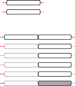
RRA: Rotate right (accumulator)
TODO
Opcode 0b00011111/0x1F Duration 1 machine cycle
Length 1 byte: opcode Flags
Z = 0, N = 0, H = 0, C = ⭐
Simple timing and pseudocode
Mem R/W
M-cycle
opcode
M1
Detailed timing and pseudocode
Misc op
ALU op
IDU op
Data bus
Addr bus
M-cycle
Previous
Previous A ← rr A
Previous PC ← PC + 1
IR ← mem IR ← mem
Previous PC
M1 M2/M1
TODO
86

RLC r: Rotate left circular (register)
TODO
Opcode 0b00000xxx/various Duration 2 machine cycles
Length 2 bytes: CB prefix + opcode Flags
Z = ⭐, N = 0, H = 0, C = ⭐
Simple timing and pseudocode
Mem R/W
M-cycle
CB prefix opcode
M1 M2
Detailed timing and pseudocode
Misc op
ALU op
IDU op
Data bus
Addr bus
M-cycle
Previous
Previous r ← rlc r
Previous PC ← PC + 1 PC ← PC + 1
IR ← mem IR ← mem IR ← mem
Previous PC PC
M1 M2 M3/M1
TODO
87

RLC (HL): Rotate left circular (indirect HL)
TODO
Opcode
0x06
Duration 4 machine cycles
Length 2 bytes: CB prefix + opcode Flags
Z = ⭐, N = 0, H = 0, C = ⭐
Simple timing and pseudocode
Mem R/W
M-cycle
CB prefix opcode R: data W: data
M1 M2 M3 M4
Detailed timing and pseudocode
Misc op
ALU op
IDU op
Data bus
Addr bus
M-cycle
Previous
Previous mem ← rlc Z
Previous PC ← PC + 1 PC ← PC + 1
IR ← mem IR ← mem Z ← mem mem ← ALU IR ← mem
Previous PC HL HL PC
M1 M2 M3 M4 M5/M1
TODO
88

RRC r: Rotate right circular (register)
TODO
Opcode 0b00001xxx/various Duration 2 machine cycles
Length 2 bytes: CB prefix + opcode Flags
Z = ⭐, N = 0, H = 0, C = ⭐
Simple timing and pseudocode
Mem R/W
M-cycle
CB prefix opcode
M1 M2
Detailed timing and pseudocode
Misc op
ALU op
IDU op
Data bus
Addr bus
M-cycle
Previous
Previous r ← rrc r
Previous PC ← PC + 1 PC ← PC + 1
IR ← mem IR ← mem IR ← mem
Previous PC PC
M1 M2 M3/M1
TODO
89

RRC (HL): Rotate right circular (indirect HL)
TODO
Opcode
0x0E
Duration 4 machine cycles
Length 2 bytes: CB prefix + opcode Flags
Z = ⭐, N = 0, H = 0, C = ⭐
Simple timing and pseudocode
Mem R/W
M-cycle
CB prefix opcode R: data W: data
M1 M2 M3 M4
Detailed timing and pseudocode
Misc op
ALU op
IDU op
Data bus
Addr bus
M-cycle
Previous
Previous mem ← rrc Z
Previous PC ← PC + 1 PC ← PC + 1
IR ← mem IR ← mem Z ← mem mem ← ALU IR ← mem
Previous PC HL HL PC
M1 M2 M3 M4 M5/M1
TODO
90

RL r: Rotate left (register)
TODO
Opcode 0b00010xxx/various Duration 2 machine cycles
Length 2 bytes: CB prefix + opcode Flags
Z = ⭐, N = 0, H = 0, C = ⭐
Simple timing and pseudocode
Mem R/W
M-cycle
CB prefix opcode
M1 M2
Detailed timing and pseudocode
Misc op
ALU op
IDU op
Data bus
Addr bus
M-cycle
Previous
Previous r ← rl r
Previous PC ← PC + 1 PC ← PC + 1
IR ← mem IR ← mem IR ← mem
Previous PC PC
M1 M2 M3/M1
TODO
91

RL (HL): Rotate left (indirect HL)
TODO
Opcode
0x16
Duration 4 machine cycles
Length 2 bytes: CB prefix + opcode Flags
Z = ⭐, N = 0, H = 0, C = ⭐
Simple timing and pseudocode
Mem R/W
M-cycle
CB prefix opcode R: data W: data
M1 M2 M3 M4
Detailed timing and pseudocode
Misc op
ALU op
IDU op
Data bus
Addr bus
M-cycle
Previous
Previous mem ← rl Z
Previous PC ← PC + 1 PC ← PC + 1
IR ← mem IR ← mem Z ← mem mem ← ALU IR ← mem
Previous PC HL HL PC
M1 M2 M3 M4 M5/M1
TODO
92

RR r: Rotate right (register)
TODO
Opcode 0b00011xxx/various Duration 2 machine cycles
Length 2 bytes: CB prefix + opcode Flags
Z = ⭐, N = 0, H = 0, C = ⭐
Simple timing and pseudocode
Mem R/W
M-cycle
CB prefix opcode
M1 M2
Detailed timing and pseudocode
Misc op
ALU op
IDU op
Data bus
Addr bus
M-cycle
Previous
Previous r ← rr r
Previous PC ← PC + 1 PC ← PC + 1
IR ← mem IR ← mem IR ← mem
Previous PC PC
M1 M2 M3/M1
TODO
93

RR (HL): Rotate right (indirect HL)
TODO
Opcode
0x1E
Duration 4 machine cycles
Length 2 bytes: CB prefix + opcode Flags
Z = ⭐, N = 0, H = 0, C = ⭐
Simple timing and pseudocode
Mem R/W
M-cycle
CB prefix opcode R: data W: data
M1 M2 M3 M4
Detailed timing and pseudocode
Misc op
ALU op
IDU op
Data bus
Addr bus
M-cycle
Previous
Previous mem ← rr Z
Previous PC ← PC + 1 PC ← PC + 1
IR ← mem IR ← mem Z ← mem mem ← ALU IR ← mem
Previous PC HL HL PC
M1 M2 M3 M4 M5/M1
TODO
94

SLA r: Shift left arithmetic (register)
TODO
Opcode 0b00100xxx/various Duration 2 machine cycles
Length 2 bytes: CB prefix + opcode Flags
Z = ⭐, N = 0, H = 0, C = ⭐
Simple timing and pseudocode
Mem R/W
M-cycle
CB prefix opcode
M1 M2
Detailed timing and pseudocode
Misc op
ALU op
IDU op
Data bus
Addr bus
M-cycle
Previous
Previous r ← sla r
Previous PC ← PC + 1 PC ← PC + 1
IR ← mem IR ← mem IR ← mem
Previous PC PC
M1 M2 M3/M1
TODO
95

SLA (HL): Shift left arithmetic (indirect HL)
TODO
Opcode
0x26
Duration 4 machine cycles
Length 2 bytes: CB prefix + opcode Flags
Z = ⭐, N = 0, H = 0, C = ⭐
Simple timing and pseudocode
Mem R/W
M-cycle
CB prefix opcode R: data W: data
M1 M2 M3 M4
Detailed timing and pseudocode
Misc op
ALU op
IDU op
Data bus
Addr bus
M-cycle
Previous
Previous mem ← sla Z
Previous PC ← PC + 1 PC ← PC + 1
IR ← mem IR ← mem Z ← mem mem ← ALU IR ← mem
Previous PC HL HL PC
M1 M2 M3 M4 M5/M1
TODO
96

SRA r: Shift right arithmetic (register)
TODO
Opcode 0b00101xxx/various Duration 2 machine cycles
Length 2 bytes: CB prefix + opcode Flags
Z = ⭐, N = 0, H = 0, C = ⭐
Simple timing and pseudocode
Mem R/W
M-cycle
CB prefix opcode
M1 M2
Detailed timing and pseudocode
Misc op
ALU op
IDU op
Data bus
Addr bus
M-cycle
Previous
Previous r ← sra r
Previous PC ← PC + 1 PC ← PC + 1
IR ← mem IR ← mem IR ← mem
Previous PC PC
M1 M2 M3/M1
TODO
97

SRA (HL): Shift right arithmetic (indirect HL)
TODO
Opcode
0x2E
Duration 4 machine cycles
Length 2 bytes: CB prefix + opcode Flags
Z = ⭐, N = 0, H = 0, C = ⭐
Simple timing and pseudocode
Mem R/W
M-cycle
CB prefix opcode R: data W: data
M1 M2 M3 M4
Detailed timing and pseudocode
Misc op
ALU op
IDU op
Data bus
Addr bus
M-cycle
Previous
Previous mem ← sra Z
Previous PC ← PC + 1 PC ← PC + 1
IR ← mem IR ← mem Z ← mem mem ← ALU IR ← mem
Previous PC HL HL PC
M1 M2 M3 M4 M5/M1
TODO
98

SWAP r: Swap nibbles (register)
TODO
Opcode 0b00110xxx/various Duration 2 machine cycles
Length 2 bytes: CB prefix + opcode Flags
Z = ⭐, N = 0, H = 0, C = 0
Simple timing and pseudocode
Mem R/W
M-cycle
CB prefix opcode
M1 M2
Detailed timing and pseudocode
Misc op
ALU op
IDU op
Data bus
Addr bus
M-cycle
Previous
Previous r ← swap r
Previous PC ← PC + 1 PC ← PC + 1
IR ← mem IR ← mem IR ← mem
Previous PC PC
M1 M2 M3/M1
TODO
99

SWAP (HL): Swap nibbles (indirect HL)
TODO
Opcode
0x36
Duration 4 machine cycles
Length 2 bytes: CB prefix + opcode Flags
Z = ⭐, N = 0, H = 0, C = 0
Simple timing and pseudocode
Mem R/W
M-cycle
CB prefix opcode R: data W: data
M1 M2 M3 M4
Detailed timing and pseudocode
Misc op
ALU op
IDU op
Data bus
Addr bus
M-cycle
Previous
Previous mem ← swap Z
Previous PC ← PC + 1 PC ← PC + 1
IR ← mem IR ← mem Z ← mem mem ← ALU IR ← mem
Previous PC HL HL PC
M1 M2 M3 M4 M5/M1
TODO
100

SRL r: Shift right logical (register)
TODO
Opcode 0b00111xxx/various Duration 2 machine cycles
Length 2 bytes: CB prefix + opcode Flags
Z = ⭐, N = 0, H = 0, C = ⭐
Simple timing and pseudocode
Mem R/W
M-cycle
CB prefix opcode
M1 M2
Detailed timing and pseudocode
Misc op
ALU op
IDU op
Data bus
Addr bus
M-cycle
Previous
Previous r ← srl r
Previous PC ← PC + 1 PC ← PC + 1
IR ← mem IR ← mem IR ← mem
Previous PC PC
M1 M2 M3/M1
TODO
101

SRL (HL): Shift right logical (indirect HL)
TODO
Opcode
0x3E
Duration 4 machine cycles
Length 2 bytes: CB prefix + opcode Flags
Z = ⭐, N = 0, H = 0, C = ⭐
Simple timing and pseudocode
Mem R/W
M-cycle
CB prefix opcode R: data W: data
M1 M2 M3 M4
Detailed timing and pseudocode
Misc op
ALU op
IDU op
Data bus
Addr bus
M-cycle
Previous
Previous mem ← srl Z
Previous PC ← PC + 1 PC ← PC + 1
IR ← mem IR ← mem Z ← mem mem ← ALU IR ← mem
Previous PC HL HL PC
M1 M2 M3 M4 M5/M1
TODO
102

BIT b, r: Test bit (register)
TODO
Opcode 0b01xxxxxx/various Duration 2 machine cycles
Length 2 bytes: CB prefix + opcode Flags
Z = ⭐, N = 0, H = 1
Simple timing and pseudocode
Mem R/W
M-cycle
CB prefix opcode
M1 M2
Detailed timing and pseudocode
Misc op
ALU op
IDU op
Data bus
Addr bus
M-cycle
Previous
Previous bit b, r
Previous PC ← PC + 1 PC ← PC + 1
IR ← mem IR ← mem IR ← mem
Previous PC PC
M1 M2 M3/M1
TODO
103

BIT b, (HL): Test bit (indirect HL)
TODO
Opcode 0b01xxx110/various Duration 3 machine cycles
Length 2 bytes: CB prefix + opcode Flags
Z = ⭐, N = 0, H = 1
Simple timing and pseudocode
Mem R/W
M-cycle
CB prefix opcode R: data
M1 M2 M3
Detailed timing and pseudocode
Misc op
ALU op
IDU op
Data bus
Addr bus
M-cycle
Previous
Previous bit b, Z
Previous PC ← PC + 1 PC ← PC + 1
IR ← mem IR ← mem Z ← mem IR ← mem
Previous PC HL PC
M1 M2 M3 M4/M1
TODO
104

RES b, r: Reset bit (register)
TODO
Opcode 0b10xxxxxx/various Duration 2 machine cycles
Length 2 bytes: CB prefix + opcode Flags -
Simple timing and pseudocode
Mem R/W
M-cycle
CB prefix opcode
M1 M2
Detailed timing and pseudocode
Misc op
ALU op
IDU op
Data bus
Addr bus
M-cycle
Previous
Previous r ← res b, r
Previous PC ← PC + 1 PC ← PC + 1
IR ← mem IR ← mem IR ← mem
Previous PC PC
M1 M2 M3/M1
TODO
105

RES b, (HL): Reset bit (indirect HL)
TODO
Opcode 0b10xxx110/various Duration 4 machine cycles
Length 2 bytes: CB prefix + opcode Flags -
Simple timing and pseudocode
Mem R/W
M-cycle
CB prefix opcode R: data W: data
M1 M2 M3 M4
Detailed timing and pseudocode
Misc op
ALU op
IDU op
Data bus
Addr bus
M-cycle
Previous
Previous mem ← res b, Z
Previous PC ← PC + 1 PC ← PC + 1
IR ← mem IR ← mem Z ← mem mem ← ALU IR ← mem
Previous PC HL HL PC
M1 M2 M3 M4 M5/M1
TODO
106

SET b, r: Set bit (register)
TODO
Opcode 0b11xxxxxx/various Duration 2 machine cycles
Length 2 bytes: CB prefix + opcode Flags -
Simple timing and pseudocode
Mem R/W
M-cycle
CB prefix opcode
M1 M2
Detailed timing and pseudocode
Misc op
ALU op
IDU op
Data bus
Addr bus
M-cycle
Previous
Previous r ← set b, r
Previous PC ← PC + 1 PC ← PC + 1
IR ← mem IR ← mem IR ← mem
Previous PC PC
M1 M2 M3/M1
TODO
107

SET b, (HL): Set bit (indirect HL)
TODO
Opcode 0b11xxx110/various Duration 4 machine cycles
Length 2 bytes: CB prefix + opcode Flags -
Simple timing and pseudocode
Mem R/W
M-cycle
CB prefix opcode R: data W: data
M1 M2 M3 M4
Detailed timing and pseudocode
Misc op
ALU op
IDU op
Data bus
Addr bus
M-cycle
Previous
Previous mem ← set b, Z
Previous PC ← PC + 1 PC ← PC + 1
IR ← mem IR ← mem Z ← mem mem ← ALU IR ← mem
Previous PC HL HL PC
M1 M2 M3 M4 M5/M1
TODO
108
109

6.7 Control flow instructions
JP nn: Jump
Unconditional jump to the absolute address specified by the 16-bit immediate operand nn.
Opcode 0b11000011/0xC3 Duration 4 machine cycles
Length 3 bytes: opcode + LSB(nn) + MSB(nn) Flags -
Simple timing and pseudocode
Mem R/W
M-cycle
opcode R: lsb(nn) R: msb(nn)
M1 M2 M3 M4
opcode = read_memory(addr=PC); PC = PC + 1
if opcode == 0xC3:
nn_lsb = read_memory(addr=PC); PC = PC + 1
nn_msb = read_memory(addr=PC); PC = PC + 1
nn = unsigned_16(lsb=nn_lsb, msb=nn_msb)
PC = nn
Detailed timing and pseudocode
Misc op
ALU op
IDU op
Data bus
Addr bus
M-cycle
Previous PC ← WZ
Previous
Previous PC ← PC + 1 PC ← PC + 1 PC ← PC + 1
IR ← mem Z ← mem W ← mem IR ← mem
Previous PC PC
0x0000
PC
M1 M2 M3 M4 M5/M1
# M2
if IR == 0xC3:
Z = read_memory(addr=PC); PC = PC + 1
# M3
W = read_memory(addr=PC); PC = PC + 1
# M4
PC = WZ
# M5/M1
IR, intr = fetch_cycle(addr=PC); PC = PC + 1
110

JP HL: Jump to HL
Unconditional jump to the absolute address specified by the 16-bit register HL.
Opcode 0b11101001/0xE9 Duration 1 machine cycle
Length 1 byte: opcode Flags -
Simple timing and pseudocode
Mem R/W
M-cycle
opcode
M1
opcode = read_memory(addr=PC); PC = PC + 1
if opcode == 0xE9:
PC = HL
Detailed timing and pseudocode
Misc op
ALU op
IDU op
Data bus
Addr bus
M-cycle
Previous
Previous
Previous PC ← HL + 1
IR ← mem IR ← mem
Previous HL
M1 M2/M1
# M2/M1
if IR == 0xE9:
IR, intr = fetch_cycle(addr=HL); PC = HL + 1
111

Warning
In some documentation this instruction is written as JP [HL]. This is very misleading,
since brackets are usually used to indicate a memory read, and this instruction simply
copies the value of HL to PC.
JP cc, nn: Jump (conditional)
Conditional jump to the absolute address specified by the 16-bit operand nn, depending on the
condition cc.
Note that the operand (absolute address) is read even when the condition is false!
Opcode 0b110xx010/various Duration 4 machine cycles (cc=true)
3 machine cycles (cc=false)
Length 3 bytes: opcode + LSB(nn) + MSB(nn) Flags -
Simple timing and pseudocode
cc=true
Mem R/W
M-cycle
opcode R: lsb(nn) R: msb(nn)
M1 M2 M3 M4
cc=false
Mem R/W
M-cycle
opcode R: lsb(nn) R: msb(nn)
M1 M2 M3
opcode = read_memory(addr=PC); PC = PC + 1
if opcode == 0xC2: # example: JP NZ, nn
nn_lsb = read_memory(addr=PC); PC = PC + 1
nn_msb = read_memory(addr=PC); PC = PC + 1
nn = unsigned_16(lsb=nn_lsb, msb=nn_msb)
if !flags.Z: # cc=true
PC = nn
112

Detailed timing and pseudocode
cc=true
Misc op
ALU op
IDU op
Data bus
Addr bus
M-cycle
Previous cc check PC ← WZ
Previous
Previous PC ← PC + 1 PC ← PC + 1 PC ← PC + 1
IR ← mem Z ← mem W ← mem IR ← mem
Previous PC PC
0x0000
PC
M1 M2 M3 M4 M5/M1
cc=false
Misc op
ALU op
IDU op
Data bus
Addr bus
M-cycle
Previous cc check
Previous
Previous PC ← PC + 1 PC ← PC + 1 PC ← PC + 1
IR ← mem Z ← mem W ← mem IR ← mem
Previous PC PC PC
M1 M2 M3 M4/M1
# M2
if IR == 0xC2: # example: JP NZ, nn
Z = read_memory(addr=PC); PC = PC + 1
# M3
W = read_memory(addr=PC); PC = PC + 1
if !flags.Z: # cc=true
# M4
PC = WZ
# M5/M1
IR, intr = fetch_cycle(addr=PC); PC = PC + 1
else: # cc=false
# M4/M1
IR, intr = fetch_cycle(addr=PC); PC = PC + 1
113

JR e: Relative jump
Unconditional jump to the relative address specified by the signed 8-bit operand e.
Opcode 0b00011000/0x18 Duration 3 machine cycles
Length 2 bytes: opcode + e Flags -
Simple timing and pseudocode
Mem R/W
M-cycle
opcode R: e
M1 M2 M3
opcode = read_memory(addr=PC); PC = PC + 1
if opcode == 0x18:
e = signed_8(read_memory(addr=PC)); PC = PC + 1
PC = PC + e
Detailed timing and pseudocode
Misc op
ALU op
IDU op
Data bus
Addr bus
M-cycle
Previous
Previous Z ← PCL + Z
Previous PC ← PC + 1 W ← adj PCH PC ← WZ + 1
IR ← mem Z ← mem ALU IR ← mem
Previous PC PCH WZ
M1 M2 M3 M4/M1
# M2
if IR == 0x18:
Z = read_memory(addr=PC); PC = PC + 1
# M3
Z_sign = bit(7, Z)
result, carry_per_bit = Z + lsb(PC)
Z = result
adj = 1 if carry_per_bit[7] and not Z_sign else
-1 if not carry_per_bit[7] and Z_sign else
0
W = msb(PC) + adj
# M4/M1
IR, intr = fetch_cycle(addr=WZ); PC = WZ + 1
114

JR cc, e: Relative jump (conditional)
Conditional jump to the relative address specified by the signed 8-bit operand e, depending on
the condition cc.
Note that the operand (relative address offset) is read even when the condition is false!
Opcode 0b001xx000/various Duration 3 machine cycles (cc=true)
2 machine cycles (cc=false)
Length 2 bytes: opcode + e Flags -
Simple timing and pseudocode
cc=true
Mem R/W
M-cycle
opcode R: e
M1 M2 M3
cc=false
Mem R/W
M-cycle
opcode R: e
M1 M2
opcode = read_memory(addr=PC); PC = PC + 1
if opcode == 0x20:
e = signed_8(read_memory(addr=PC)); PC = PC + 1
if !flags.Z: # cc=true
PC = PC + e
115

Detailed timing and pseudocode
cc=true
Misc op
ALU op
IDU op
Data bus
Addr bus
M-cycle
Previous cc check
Previous Z ← PCL + Z
Previous PC ← PC + 1 W ← adj PCH PC ← WZ + 1
IR ← mem Z ← mem ALU IR ← mem
Previous PC PCH WZ
M1 M2 M3 M4/M1
cc=false
Misc op
ALU op
IDU op
Data bus
Addr bus
M-cycle
Previous cc check
Previous
Previous PC ← PC + 1 PC ← PC + 1
IR ← mem Z ← mem IR ← mem
Previous PC PC
M1 M2 M3/M1
# M2
if IR == 0x20:
Z = read_memory(addr=PC); PC = PC + 1
if !flags.Z: # cc=true
# M3
Z_sign = bit(7, Z)
result, carry_per_bit = Z + lsb(PC)
Z = result
adj = 1 if carry_per_bit[7] and not Z_sign else
-1 if not carry_per_bit[7] and Z_sign else
0
W = msb(PC) + adj
# M4/M1
IR, intr = fetch_cycle(addr=WZ); PC = WZ + 1
else: # cc=false
# M3/M1
IR, intr = fetch_cycle(addr=PC); PC = PC + 1
116

CALL nn: Call function
Unconditional function call to the absolute address specified by the 16-bit operand nn.
Opcode 0b11001101/0xCD Duration 6 machine cycles
Length 3 bytes: opcode + LSB(nn) + MSB(nn) Flags -
Simple timing and pseudocode
Mem R/W
M-cycle
opcode R: lsb(nn) R: msb(nn) W: msb(PC₀+3) W: lsb(PC₀+3)
M1 M2 M3 M4 M5 M6
opcode = read_memory(addr=PC); PC = PC + 1
if opcode == 0xCD:
nn_lsb = read_memory(addr=PC); PC = PC + 1
nn_msb = read_memory(addr=PC); PC = PC + 1
nn = unsigned_16(lsb=nn_lsb, msb=nn_msb)
SP = SP - 1
write_memory(addr=SP, data=msb(PC)); SP = SP - 1
write_memory(addr=SP, data=lsb(PC))
PC = nn
Detailed timing and pseudocode
Misc op
ALU op
IDU op
Data bus
Addr bus
M-cycle
Previous PC ← WZ
Previous
Previous PC ← PC + 1 PC ← PC + 1 SP ← SP - 1 SP ← SP - 1 SP ← SP PC ← PC + 1
IR ← mem Z ← mem W ← mem mem ← PCH mem ← PCL IR ← mem
Previous PC PC SP SP SP PC
M1 M2 M3 M4 M5 M6 M7/M1
# M2
if IR == 0xCD:
Z = read_memory(addr=PC); PC = PC + 1
# M3
W = read_memory(addr=PC); PC = PC + 1
# M4
SP = SP - 1
# M5
write_memory(addr=SP, data=msb(PC)); SP = SP - 1
# M6
write_memory(addr=SP, data=lsb(PC)); PC = WZ
# M7/M1
IR, intr = fetch_cycle(addr=PC); PC = PC + 1
117

CALL cc, nn: Call function (conditional)
Conditional function call to the absolute address specified by the 16-bit operand nn, depending
on the condition cc.
Note that the operand (absolute address) is read even when the condition is false!
Opcode 0b110xx100/various Duration 6 machine cycles (cc=true)
3 machine cycles (cc=false)
Length 3 bytes: opcode + LSB(nn) + MSB(nn) Flags -
Simple timing and pseudocode
cc=true
Mem R/W
M-cycle
opcode R: lsb(nn) R: msb(nn) W: msb(PC₀+3) W: lsb(PC₀+3)
M1 M2 M3 M4 M5 M6
cc=false
Mem R/W
M-cycle
opcode R: lsb(nn) R: msb(nn)
M1 M2 M3
opcode = read_memory(addr=PC); PC = PC + 1
if opcode == 0xC4: # example: CALL NZ, nn
nn_lsb = read_memory(addr=PC); PC = PC + 1
nn_msb = read_memory(addr=PC); PC = PC + 1
nn = unsigned_16(lsb=nn_lsb, msb=nn_msb)
if !flags.Z: # cc=true
SP = SP - 1
write_memory(addr=SP, data=msb(PC)); SP = SP - 1
write_memory(addr=SP, data=lsb(PC))
PC = nn
118

Detailed timing and pseudocode
cc=true
Misc op
ALU op
IDU op
Data bus
Addr bus
M-cycle
Previous cc check PC ← WZ
Previous
Previous PC ← PC + 1 PC ← PC + 1 SP ← SP - 1 SP ← SP - 1 SP ← SP PC ← PC + 1
IR ← mem Z ← mem W ← mem mem ← PCH mem ← PCL IR ← mem
Previous PC PC SP SP SP PC
M1 M2 M3 M4 M5 M6 M7/M1
cc=false
Misc op
ALU op
IDU op
Data bus
Addr bus
M-cycle
Previous cc check
Previous
Previous PC ← PC + 1 PC ← PC + 1 PC ← PC + 1
IR ← mem Z ← mem W ← mem IR ← mem
Previous PC PC PC
M1 M2 M3 M4/M1
# M2
if IR == 0xC4: # example: CALL NZ, nn
Z = read_memory(addr=PC); PC = PC + 1
# M3
W = read_memory(addr=PC); PC = PC + 1
if !flags.Z: # cc=true
# M4
SP = SP - 1
# M5
write_memory(addr=SP, data=msb(PC)); SP = SP - 1
# M6
write_memory(addr=SP, data=lsb(PC)); PC = WZ
# M7/M1
IR, intr = fetch_cycle(addr=PC); PC = PC + 1
else: # cc=false
# M4/M1
IR, intr = fetch_cycle(addr=PC); PC = PC + 1
119

RET: Return from function
Unconditional return from a function.
Opcode 0b11001001/0xC9 Duration 4 machine cycles
Length 1 byte: opcode Flags -
Simple timing and pseudocode
Mem R/W
M-cycle
opcode R: lsb(PC) R: msb(PC)
M1 M2 M3 M4
opcode = read_memory(addr=PC); PC = PC + 1
if opcode == 0xC9:
lsb = read_memory(addr=SP); SP = SP + 1
msb = read_memory(addr=SP); SP = SP + 1
PC = unsigned_16(lsb=lsb, msb=msb)
Detailed timing and pseudocode
Misc op
ALU op
IDU op
Data bus
Addr bus
M-cycle
Previous PC ← WZ
Previous
Previous SP ← SP + 1 SP ← SP + 1 PC ← PC + 1
IR ← mem Z ← mem W ← mem IR ← mem
Previous SP SP
0x0000
PC
M1 M2 M3 M4 M5/M1
# M2
if IR == 0xC9:
Z = read_memory(addr=SP); SP = SP + 1
# M3
W = read_memory(addr=SP); SP = SP + 1
# M4
PC = WZ
# M5/M1
IR, intr = fetch_cycle(addr=PC); PC = PC + 1
120

RET cc: Return from function (conditional)
Conditional return from a function, depending on the condition cc.
Opcode 0b110xx000/various Duration 5 machine cycles (cc=true)
2 machine cycles (cc=false)
Length 1 byte: opcode Flags -
Simple timing and pseudocode
cc=true
Mem R/W
M-cycle
opcode R: lsb(PC) R: msb(PC)
M1 M2 M3 M4 M5
cc=false
Mem R/W
M-cycle
opcode
M1 M2
opcode = read_memory(addr=PC); PC = PC + 1
if opcode == 0xC0: # example: RET NZ
if !flags.Z: # cc=true
lsb = read_memory(addr=SP); SP = SP + 1
msb = read_memory(addr=SP); SP = SP + 1
PC = unsigned_16(lsb=lsb, msb=msb)
Detailed timing and pseudocode
cc=true
Misc op
ALU op
IDU op
Data bus
Addr bus
M-cycle
Previous cc check PC ← WZ
Previous
Previous SP ← SP + 1 SP ← SP + 1 PC ← PC + 1
IR ← mem Z ← mem W ← mem IR ← mem
Previous
0x0000
SP SP
0x0000
PC
M1 M2 M3 M4 M5 M6/M1
cc=false
Misc op
ALU op
IDU op
Data bus
Addr bus
M-cycle
Previous cc check
Previous
Previous PC ← PC + 1
IR ← mem IR ← mem
Previous
0x0000
PC
M1 M2 M3/M1
# M2
if IR == 0xC0: # example: RET NZ
if !flags.Z: # cc=true
# M3
Z = read_memory(addr=SP); SP = SP + 1
# M4
W = read_memory(addr=SP); SP = SP + 1
# M5
PC = WZ
# M6/M1
IR, intr = fetch_cycle(addr=PC); PC = PC + 1
else: # cc=false
# M3
IR, intr = fetch_cycle(addr=PC); PC = PC + 1
121

RETI: Return from interrupt handler
Unconditional return from a function. Also enables interrupts by setting IME=1.
Opcode 0b11011001/0xD9 Duration 4 machine cycles
Length 1 byte: opcode Flags -
Simple timing and pseudocode
Mem R/W
M-cycle
opcode R: lsb(PC) R: msb(PC)
M1 M2 M3 M4
opcode = read_memory(addr=PC); PC = PC + 1
if opcode == 0xD9:
lsb = read_memory(addr=SP); SP = SP + 1
msb = read_memory(addr=SP); SP = SP + 1
PC = unsigned_16(lsb=lsb, msb=msb)
IME = 1
Detailed timing and pseudocode
Misc op
ALU op
IDU op
Data bus
Addr bus
M-cycle
Previous PC ← WZ, IME ← 1
Previous
Previous SP ← SP + 1 SP ← SP + 1 PC ← PC + 1
IR ← mem Z ← mem W ← mem IR ← mem
Previous SP SP
0x0000
PC
M1 M2 M3 M4 M5/M1
# M2
if IR == 0xD9:
Z = read_memory(addr=SP); SP = SP + 1
# M3
W = read_memory(addr=SP); SP = SP + 1
# M4
PC = WZ; IME = 1
# M5/M1
IR, intr = fetch_cycle(addr=PC); PC = PC + 1
122
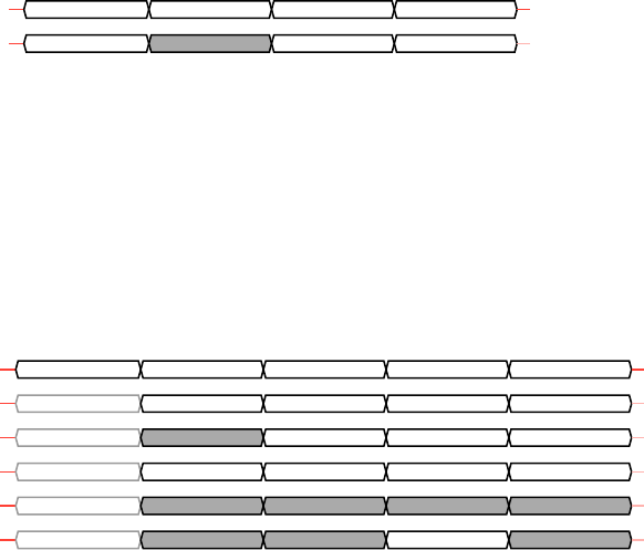
RST n: Restart / Call function (implied)
Unconditional function call to the absolute fixed address defined by the opcode.
Opcode 0b11xxx111/various Duration 4 machine cycles
Length 1 byte: opcode Flags -
Simple timing and pseudocode
Mem R/W
M-cycle
opcode W: msb PC W: lsb PC
M1 M2 M3 M4
opcode = read_memory(addr=PC); PC = PC + 1
if opcode == 0xDF: # example: RST 0x18
n = 0x18
SP = SP - 1
write_memory(addr=SP, data=msb(PC)); SP = SP - 1
write_memory(addr=SP, data=lsb(PC))
PC = unsigned_16(lsb=n, msb=0x00)
Detailed timing and pseudocode
Misc op
ALU op
IDU op
Data bus
Addr bus
M-cycle
Previous PC ← addr
Previous
Previous SP ← SP - 1 SP ← SP - 1 SP ← SP PC ← PC + 1
IR ← mem mem ← PCH mem ← PCL IR ← mem
Previous SP SP SP PC
M1 M2 M3 M4 M5/M1
# M2
if IR == 0xDF: # example: RST 0x18
SP = SP - 1
# M3
write_memory(addr=SP, data=msb(PC)); SP = SP - 1
# M4
write_memory(addr=SP, data=lsb(PC)); PC = 0x0018
# M5/M1
IR, intr = fetch_cycle(addr=PC); PC = PC + 1
123

6.8 Miscellaneous instructions
HALT: Halt system clock
TODO
STOP: Stop system and main clocks
TODO
DI: Disable interrupts
Disables interrupt handling by setting IME=0 and cancelling any scheduled effects of the EI
instruction if any.
Opcode 0b11110011/0xF3 Duration 1 machine cycle
Length 1 byte: opcode Flags -
Simple timing and pseudocode
Mem R/W
M-cycle
opcode
M1
opcode = read_memory(addr=PC); PC = PC + 1
if opcode == 0xF3:
IME = 0
Detailed timing and pseudocode
Misc op
ALU op
IDU op
Data bus
Addr bus
M-cycle
Previous IME ← 0
Previous
Previous PC ← PC + 1
IR ← mem IR ← mem
Previous PC
M1 M2/M1
# M2/M1
if IR == 0xF3:
# interrupt checking is suppressed so fetch_cycle(..) is not used
IR = read_memory(addr=PC); PC = PC + 1; IME = 0
124

EI: Enable interrupts
Schedules interrupt handling to be enabled after the next machine cycle.
Opcode 0b11111011/0xFB Duration 1 machine cycle
Length 1 byte: opcode Flags -
Simple timing and pseudocode
Mem R/W
M-cycle
opcode
M1
opcode = read_memory(addr=PC); PC = PC + 1
if opcode == 0xFB:
IME_next = 1
Detailed timing and pseudocode
Misc op
ALU op
IDU op
Data bus
Addr bus
M-cycle
Previous IME ← 1
Previous
Previous PC ← PC + 1
IR ← mem IR ← mem
Previous PC
M1 M2/M1
# M2/M1
if IR == 0xFB:
IR, intr = fetch_cycle(addr=PC); PC = PC + 1; IME = 1
125
NOP: No operation
No operation. This instruction doesn’t do anything, but can be used to add a delay of one ma-
chine cycle and increment PC by one.
Opcode 0b00000000/0x00 Duration 1 machine cycle
Length 1 byte: opcode Flags -
Simple timing and pseudocode
Mem R/W
M-cycle
opcode
M1
opcode = read_memory(addr=PC); PC = PC + 1
if opcode == 0x00:
# nothing
Detailed timing and pseudocode
Misc op
ALU op
IDU op
Data bus
Addr bus
M-cycle
Previous
Previous
Previous PC ← PC + 1
IR ← mem IR ← mem
Previous PC
M1 M2/M1
# M2/M1
if IR == 0x00:
IR, intr = fetch_cycle(addr=PC); PC = PC + 1
126
127
Part III
Game Boy SoC peripherals and features
128

Chapter 7
Boot ROM
The Game Boy SoC includes a small embedded boot ROM, which can be mapped to the
0x0000-0x00FF memory area. While mapped, all reads from this area are handled by the boot
ROM instead of the external cartridge, and all writes to this area are ignored and cannot be
seen by external hardware (e.g. the cartridge MBC).
The boot ROM is enabled by default, so when the system exits the reset state and the CPU
starts execution from address 0x0000, it executes the boot ROM instead of instructions from
the cartridge ROM. The boot ROM is responsible for showing the initial logo, and checking that
a valid cartridge is inserted into the system. If the cartridge is valid, the boot ROM unmaps itself
before execution of the cartridge ROM starts at 0x0100. The cartridge ROM has no chance of
executing any instructions before the boot ROM is unmapped, which prevents the boot ROM
from being read byte by byte in normal conditions.
Warning
Don’t confuse the boot ROM with the additional SNES ROM in SGB/SGB2 that is executed
by the SNES CPU.
Register7.1: 0xFF50 - BOOT - Boot ROM lock register
U U U U U U U R/W-0
BOOT_OFF
bit 7 6 5 4 3 2 1 bit 0
bit 7-1 Unimplemented: Ignored during writes, reads are undefined
bit 0 BOOT_OFF: Boot ROM lock bit
0b1 = Boot ROM is disabled and 0x0000-0x00FF works normally.
0b0 = Boot ROM is active and intercepts accesses to 0x0000-0x00FF.
BOOT_OFF can only transition from 0b0 to 0b1, so once 0b1 has been written, the boot
ROM is permanently disabled until the next system reset. Writing 0b0 when BOOT_OFF
is 0b0 has no effect and doesn’t lock the boot ROM.
The 1-bit BOOT register controls mapping of the boot ROM. Once 0b1 has been written to it to
unmap the boot ROM, it can only be mapped again by resetting the system.
7.1 Boot ROM types
129

Type CRC32 MD5 SHA1
DMG
59c8598e 32fbbd84168d3482956eb3c5051637f5 4ed31ec6b0b175bb109c0eb5fd3d193da823339f
MGB
e6920754 71a378e71ff30b2d8a1f02bf5c7896aa 4e68f9da03c310e84c523654b9026e51f26ce7f0
SGB
ec8a83b9 d574d4f9c12f305074798f54c091a8b4 aa2f50a77dfb4823da96ba99309085a3c6278515
SGB2
53d0dd63 e0430bca9925fb9882148fd2dc2418c1 93407ea10d2f30ab96a314d8eca44fe160aea734
DMG0
c2f5cc97 a8f84a0ac44da5d3f0ee19f9cea80a8c 8bd501e31921e9601788316dbd3ce9833a97bcbc
Table7.1: Summary of boot ROM file hashes
DMG boot ROM
The most common boot ROM is the DMG boot ROM used in almost all original Game Boy units.
If a valid cartridge is inserted, the boot ROM scrolls a logo to the center of the screen, and plays
a “di-ding” sound recognizable by most people who have used Game Boy consoles.
This boot ROM was originally dumped by neviksti in 2003 by decapping the Game Boy SoC and
visually inspecting every single bit.
MGB boot ROM
This boot ROM was originally dumped by Bennvenn in 2014 by using a simple clock glitching
method that only requires one wire.
SGB boot ROM
This boot ROM was originally dumped by Costis Sideris in 2009 by using an FPGA-based clock
glitching method [4].
SGB2 boot ROM
This boot ROM was originally dumped by gekkio in 2015 by using a Teensy 3.1 -based clock
glitching method [5].
Early DMG boot ROM (“DMG0”)
Very early original Game Boy units released in Japan (often called “DMG0”) included the launch
version “DMG-CPU” SoC chip, which used a different boot ROM than later units.
This boot ROM was originally dumped by gekkio in 2016 by using a clock glitching method in-
vented by BennVenn.
130

Chapter 8
DMA (Direct Memory Access)
8.1 Object Attribute Memory (OAM) DMA
OAM DMA is a high-throughput mechanism for copying data to the OAM area (a.k.a. Object
Attribute Memory, a.k.a. sprite memory). It can copy one byte per machine cycle without in-
volving the CPU at all, which is much faster than the fastest possible memcpy routine that can be
written with the SM83 instruction set. However, a transfer cannot be cancelled and the transfer
length cannot be controlled, so the DMA transfer always updates the entire OAM area (= 160
bytes) even if you actually want to just update the first couple of bytes.
The Game Boy CPU chip contains a DMA controller that coordinates transfers between a source
area and the OAM area independently of the CPU. While a transfer is in progress, it takes con-
trol of the source bus and the OAM area, so some precaution is needed with memory accesses
(including instruction fetches) to avoid OAM DMA bus conflicts. OAM DMA uses a different
address decoding scheme than normal memory accesses, so the source bus is always either
the external bus or the video RAM bus, and the contents normally visible to the CPU in the
0xFE00-0xFFFF address range cannot be used as a source for OAM DMA transfers.
The upper 8 bits of the OAM DMA source address are stored in the DMA register, while the lower
8 bits used by both the source and target address are stored in the DMA controller and are not
accessible directly. A transfer always begins with 0x00 in the lower bits and copies exactly 160
bytes, so the lower bits are never in the 0xA0-0xFF range.
Writing to the DMA register updates the upper bits of the DMA source address and also trig-
gers an OAM DMA transfer request, although the DMA transfer does not begin immediately.
Register8.1: 0xFF46 - DMA - OAM DMA control register
R/W-x R/W-x R/W-x R/W-x R/W-x R/W-x R/W-x R/W-x
DMA<7:0>
bit 7 6 5 4 3 2 1 bit 0
bit 7-0 DMA<7:0>: OAM DMA source address
Specifies the top 8 bits of the OAM DMA source address.
Writing to this register requests an OAM DMA transfer, but it’s just a request and the
actual DMA transfer starts with a delay.
Reading this register returns the value that was previously written to the register. The
stored value is not cleared on reset, so the initial value before the first write is unknown
and should not be relied on.
Warning
Avoid writing 0xE0-0xFF to the DMA register, because some poorly designed flash carts
can trigger bus conflicts or other dangerous behaviour.
131

OAM DMA address decoding
The OAM DMA controller uses a simplified address decoding scheme, which leads to some
addresses being unusable as source addresses. Unlike normal memory accesses, OAM DMA
transfers interpret all accesses in the 0xA000-0xFFFF range as external RAM transfers. For ex-
ample, if the OAM DMA wants to read 0xFF00, it will output 0xFF00 on the external address
bus and will assert the external RAM chip select signal. The P1 register which is normally at
0xFF00 is not involved at all, because OAM DMA address decoding only uses the external bus
and the video RAM bus. Instead, the resulting behaviour depends on several factors, including
the connected cartridge. Some flash carts are not prepared for this unexpected scenario, and
a bus conflict or worse behaviour can happen.
DMA register value Used bus Asserted chip select signal
0x00-0x7F
external bus external ROM (A15)
0x80-0x9F
video RAM bus video RAM (MCS)
0xA0-0xFF
external bus external RAM (CS)
Table8.1: OAM DMA address decoding scheme
OAM DMA transfer timing
TODO
OAM DMA bus conflicts
TODO
132

Chapter 9
PPU (Picture Processing Unit)
Register9.1: 0xFF40 - LCDC - PPU control register
R/W-0 R/W-0 R/W-0 R/W-0 R/W-0 R/W-0 R/W-0 R/W-0
LCD_EN WIN_MAP WIN_EN TILE_SEL BG_MAP OBJ_SIZE OBJ_EN BG_EN
bit 7 6 5 4 3 2 1 bit 0
Register9.2: 0xFF41 - STAT - PPU status register
U R/W-0 R/W-0 R/W-0 R/W-0 R-0 R-0 R-0
INTR_LYC INTR_M2 INTR_M1 INTR_M0 LYC_STAT LCD_MODE<1:0>
bit 7 6 5 4 3 2 1 bit 0
Register9.3: 0xFF42 - SCY - Vertical scroll register
R/W-0 R/W-0 R/W-0 R/W-0 R/W-0 R/W-0 R/W-0 R/W-0
SCY<7:0>
bit 7 6 5 4 3 2 1 bit 0
Register9.4: 0xFF43 - SCX - Horizontal scroll register
R/W-0 R/W-0 R/W-0 R/W-0 R/W-0 R/W-0 R/W-0 R/W-0
SCX<7:0>
bit 7 6 5 4 3 2 1 bit 0
Register9.5: 0xFF44 - LY - Scanline register
R-0 R-0 R-0 R-0 R-0 R-0 R-0 R-0
LY<7:0>
bit 7 6 5 4 3 2 1 bit 0
Register9.6: 0xFF45 - LYC - Scanline compare register
R/W-0 R/W-0 R/W-0 R/W-0 R/W-0 R/W-0 R/W-0 R/W-0
LYC<7:0>
bit 7 6 5 4 3 2 1 bit 0
133

Chapter 10
Port P1 (Joypad, Super Game Boy communica-
tion)
Register10.1: 0xFF00 - P1 - Joypad/Super Game Boy communication register
U U W-0 W-0 R-x R-x R-x R-x
P15 P14 P13 P12 P11 P10
bit 7 6 5 4 3 2 1 bit 0
bit 7-6 Unimplemented: Ignored during writes, reads are undefined
bit 5 P15
bit 4 P14
bit 3 P13
bit 2 P12
bit 1 P11
bit 0 P10
134

Chapter 11
Serial communication
Register11.1: 0xFF01 - SB - Serial data register
R/W-0 R/W-0 R/W-0 R/W-0 R/W-0 R/W-0 R/W-0 R/W-0
SB<7:0>
bit 7 6 5 4 3 2 1 bit 0
bit 7-0 SB<7:0>: Serial data
Register11.2: 0xFF02 - SC - Serial control register
R/W-0 U U U U U U R/W-0
SIO_EN SIO_CLK
bit 7 6 5 4 3 2 1 bit 0
bit 7 SIO_EN
bit 6-1 Unimplemented: Ignored during writes, reads are undefined
bit 0 SIO_CLK
135
Part IV
Game Boy game cartridges
136

Chapter 12
MBC1 mapper chip
The majority of games for the original Game Boy use the MBC1 chip. MBC1 supports ROM sizes
up to 16 Mbit (128 banks of 0x4000 bytes) and RAM sizes up to 256 Kbit (4 banks of 0x2000
bytes). The information in this section is based on my MBC1 research, Tauwasser’s research
notes [6], and Pan Docs [7].
12.1 MBC1 registers
Caveat
These registers don’t have any standard names and are usually referred to using their
address ranges or purposes instead. This document uses names to clarify which register
is meant when referring to one.
The MBC1 chip includes four registers that affect the behaviour of the chip. Of the cartridge
bus address signals, only A13-A15 are connected to the MBC, so lower address bits don’t matter
when the CPU is accessing the MBC and all registers are effectively mapped to address ranges
instead of single addresses. All registers are smaller than 8 bits, and unused bits are simply
ignored during writes. The registers are not directly readable.
Register12.1: 0x0000-0x1FFF - RAMG - MBC1 RAM gate register
U U U U W-0 W-0 W-0 W-0
RAMG<3:0>
bit 7 6 5 4 3 2 1 bit 0
bit 7-4 Unimplemented: Ignored during writes
bit 3-0 RAMG<3:0>: RAM gate register
0b1010 = enable access to chip RAM
All other values disable access to chip RAM
The RAMG register is used to enable access to the cartridge SRAM if one exists on the car-
tridge circuit board. RAM access is disabled by default but can be enabled by writing to the
0x0000-0x1FFF address range a value with the bit pattern 0b1010 in the lower nibble. Upper
bits don’t matter, but any other bit pattern in the lower nibble disables access to RAM.
When RAM access is disabled, all writes to the external RAM area 0xA000-0xBFFF are ignored,
and reads return undefined values. Pan Docs recommends disabling RAM when it’s not being
accessed to protect the contents [7].
137

🧩 Speculation
We don’t know the physical implementation of RAMG, but it’s certainly possible that the
0b1010 bit pattern check is done at write time and the register actually consists of just a
single bit.
Register12.2: 0x2000-0x3FFF - BANK1 - MBC1 bank register 1
U U U W-0 W-0 W-0 W-0 W-1
BANK1<4:0>
bit 7 6 5 4 3 2 1 bit 0
bit 7-5 Unimplemented: Ignored during writes
bit 4-0 BANK1<4:0>: Bank register 1
Never contains the value 0b00000.
If 0b00000 is written, the resulting value will be 0b00001 instead.
The 5-bit BANK1 register is used as the lower 5 bits of the ROM bank number when the CPU
accesses the 0x4000-0x7FFF memory area.
MBC1 doesn’t allow the BANK1 register to contain zero (bit pattern 0b00000), so the initial value
at reset is 0b00001 and attempting to write 0b00000 will write 0b00001 instead. This makes it
impossible to read banks 0x00, 0x20, 0x40 and 0x60 from the 0x4000-0x7FFF memory area,
because those bank numbers have 0b00000 in the lower bits. Due to the zero value adjustment,
requesting any of these banks actually requests the next bank (e.g. 0x21 instead of 0x20).
Register12.3: 0x2000-0x3FFF - BANK1 - MBC1 bank register 2
U U U U U U W-0 W-0
BANK2<1:0>
bit 7 6 5 4 3 2 1 bit 0
bit 7-2 Unimplemented: Ignored during writes
bit 1-0 BANK2<1:0>: Bank register 2
The 2-bit BANK2 register can be used as the upper bits of the ROM bank number, or as the 2-bit
RAM bank number. Unlike BANK1, BANK2 doesn’t disallow zero, so all 2-bit values are possible.
138

Register12.4: 0x6000-0x7FFF - MODE - MBC1 mode register
U U U U U U U W-0
MODE
bit 7 6 5 4 3 2 1 bit 0
bit 7-1 Unimplemented: Ignored during writes
bit 0 MODE: Mode register
0b1 = BANK2 affects accesses to 0x0000-0x3FFF, 0x4000-0x7FFF, 0xA000-0xBFFF
0b0 = BANK2 affects only accesses to 0x4000-0x7FFF
The MODE register determines how the BANK2 register value is used during memory accesses.
Warning
Most documentation, including Pan Docs [7], calls value 0b0 ROM banking mode, and
value 0b1 RAM banking mode. This terminology reflects the common use cases, but “RAM
banking” is slightly misleading because value 0b1 also affects ROM reads in multicart
cartridges and cartridges that have a 8 or 16 Mbit ROM chip.
12.2 ROM in the 0x0000-0x7FFF area
In MBC1 cartridges, the A0-A13 cartridge bus signals are connected directly to the correspond-
ing ROM pins, and the remaining ROM pins (A14-A20) are controlled by the MBC1. These re-
maining pins form the ROM bank number.
When the 0x0000-0x3FFF address range is accessed, the effective bank number depends on
the MODE register. In MODE 0b0 the bank number is always 0, but in MODE 0b1 it’s formed by
shifting the BANK2 register value left by 5 bits.
When the 0x4000-0x7FFF addess range is accessed, the effective bank number is always a com-
bination of BANK1 and BANK2 register values.
If the cartridge ROM is smaller than 16 Mbit, there are less ROM address pins to connect to
and therefore some bank number bits are ignored. For example, 4 Mbit ROMs only need a 5-
bit bank number, so the BANK2 register value is always ignored because those bits are simply
not connected to the ROM.
ROM address bits
Accessed address Bank number Address within bank
20-19 18-14 13-0
0x0000-0x3FFF, MODE = 0b0
0b00 0b00000
A<13:0>
0x0000-0x3FFF, MODE = 0b1 BANK2
0b00000
A<13:0>
0x4000-0x7FFF
BANK2 BANK1 A<13:0>
Table12.1: Mapping of physical ROM address bits in MBC1 carts
ROM banking example 1
Let’s assume we have previously written 0x12 to the BANK1 register and 0b01 to the BANK2
register. The effective bank number during ROM reads depends on which address range we
read and on the value of the MODE register:
139
Value of the BANK 1 register
0b10010
Value of the BANK 2 register
0b01
Effective ROM bank number
(reading 0x4000-0x7FFF)
0b0110010
(= 50 = 0x32)
Effective ROM bank number
(reading 0x0000-0x3FFF, MODE = 0b0)
0b0000000
(= 0 = 0x00)
Effective ROM bank number
(reading 0x0000-0x3FFF, MODE = 0b1)
0b0100000
(= 32 = 0x20)
ROM banking example 2
Let’s assume we have previously requested ROM bank number 68, MBC1 mode is 0b0, and we
are now reading a byte from 0x72A7. The actual physical ROM address that will be read is going
to be 0x1132A7 and is constructed in the following way:
Value of the BANK 1 register
0b00100
Value of the BANK 2 register
0b10
ROM bank number
0b1000100
(= 68 = 0x44)
Address being read
0b0111 0010 1010 0111
(= 0x72A7)
Actual physical ROM address
0b1 0001 0011 0010 1010 0111
(= 0x1132A7)
12.3 RAM in the 0xA000-0xBFFF area
Some MBC1 carts include SRAM, which is mapped to the 0xA000-0xBFFF area. If no RAM is
present, or RAM is not enabled with the RAMG register, all reads return undefined values and
writes have no effect.
On boards that have RAM, the A0-A12 cartridge bus signals are connected directly to the cor-
responding RAM pins, and pins A13-A14 are controlled by the MBC1. Most of the time the RAM
size is 64 Kbit, which corresponds to a single bank of 0x2000 bytes. With larger RAM sizes the
BANK2 register value can be used for RAM banking to provide the two high address bits.
In MODE 0b0 the BANK2 register value is not used, so the first RAM bank is always mapped to
the 0xA000-0xBFFF area. In MODE 0b1 the BANK2 register value is used as the bank number.
RAM address bits
Accessed address Bank number Address within bank
14-13 12-0
0xA000-0xBFFF, MODE = 0b0 0b00 A<12:0>
0xA000-0xBFFF, MODE = 0b1 BANK2 A<12:0>
Table12.2: Mapping of physical RAM address bits in MBC1 carts
RAM banking example 1
Let’s assume we have previously written 0b10 to the BANK2 register, MODE is 0b1, RAMG is
0b1010 and we are now reading a byte from 0xB123. The actual physical RAM address that will
be read is going to be 0x5123 and is constructed in the following way:
140

Value of the BANK 2 register
0b10
Address being read
0b1011 0001 0010 0011
(= 0xB123)
Actual physical RAM address
0b101 0001 0010 0011
(= 0x5123)
12.4 MBC1 multicarts (“MBC1M”)
MBC1 is also used in a couple of “multicart” cartridges, which include more than one game on
the same cartridge. These cartridges use the same regular MBC1 chip, but the circuit board is
wired a bit differently. This alternative wiring is sometimes called “MBC1M”, but technically the
mapper chip is the same. All known MBC1 multicarts use 8 Mbit ROMs, so there’s no definitive
wiring for other ROM sizes.
In MBC1 multicarts bit 4 of the BANK1 register is not physically connected to anything, so it’s
skipped. This means that the bank number is actually a 6-bit number. In all known MBC1 multi-
carts the games reserve 16 banks each, so BANK2 can actually be considered “game number”,
while BANK1 is the internal bank number within the selected game. At reset BANK2 is 0b00,
and the “game” in this slot is actually a game selection menu. The menu code selects MODE
0b1 and writes the game number to BANK2 once the user selects a game.
From a ROM banking point of view, multicarts simply skip bit 4 of the BANK1 register, but oth-
erwise the behaviour is the same. MODE 0b1 guarantees that all ROM accesses, including ac-
cesses to 0x0000-0x3FFF, use the BANK2 register value.
ROM address bits
Accessed address Bank number Address within bank
19-18 17-14 13-0
0x0000-0x3FFF, MODE = 0b0
0b00 0b0000
A<13:0>
0x0000-0x3FFF, MODE = 0b1 BANK2
0b0000
A<13:0>
0x4000-0x7FFF
BANK2 BANK1<3:0> A<13:0>
Table12.3: Mapping of physical ROM address bits in MBC1 multicarts
ROM banking example 1
Let’s assume we have previously requested “game number” 3 (= 0b11) and ROM bank number
29 (= 0x1D), MBC1 mode is 0b1, and we are now reading a byte from 0x6C15. The actual physical
ROM address that will be read is going to be 0xF6C15 and is constructed in the following way:
Value of the BANK 1 register
0b11101
Value of the BANK 2 register
0b11
ROM bank number
0b111101
(= 61 = 0x3D)
Address being read
0b0110 1100 0001 0101
(= 0x6C15)
Actual physical ROM address
0b1111 0110 1100 0001 0101
(= 0xF6C15)
Detecting multicarts
MBC1 multicarts are not detectable by simply looking at the ROM header, because the ROM type
value is just one of the normal MBC1 values. However, detection is possible by going through
BANK2 values and looking at “bank 0” of each multicart game and doing some heuristics based
141
on the header data. All the included games, including the game selection menu, have proper
header data. One example of a good heuristic is logo data verification.
So, if you have a 8 Mbit cart with MBC1, first assume that it’s a multicart and bank numbers
are 6-bit values. Set BANK1 to zero and loop through the four possible BANK2 values while
checking the data at 0x0104-0x0133. In other words, check logo data starting from physical
ROM locations 0x00104, 0x40104, 0x80104, and 0xC0104. If proper logo data exists with most
of the BANK2 values, the cart is most likely a multicart. Note that multicarts can just have two
actual games, so one of the locations might not have the header data in place.
12.5 Dumping MBC1 carts
MBC1 cartridge dumping is fairly straightforward with the right hardware. The total number of
banks is read from the header, and each bank is read one byte at a time. However, BANK1 reg-
ister zero-adjustment and multicart cartridges need to be considered in ROM dumping code.
Banks 0x20, 0x40 and 0x60 can only be read from the 0x0000-0x3FFF memory area and only
when MODE register value is 0b1. Using MODE 0b1 has no undesirable effects when doing ROM
dumping, so using it at all times is recommended for simplicity.
Multicarts should be detected using the logo check described earlier, and if a multicart is de-
tected, BANK1 should be considered a 4-bit register in the dumping code.
BANK1 = 0x2000
BANK2 = 0x4000
MODE = 0x6000
write_byte(MODE, 0x01)
for bank in range(0, num_banks):
write_byte(BANK1, bank)
if is_multicart:
write_byte(BANK2, bank >> 4)
bank_start = 0x4000 if bank & 0x0f else 0x0000
else:
write_byte(BANK2, bank >> 5)
bank_start = 0x4000 if bank & 0x1f else 0x0000
for addr in range(bank_start, bank_start + 0x4000):
buf += read_byte(addr)
Listing12.1: Python pseudo-code for MBC1 ROM dumping
142

Chapter 13
MBC2 mapper chip
MBC2 supports ROM sizes up to 2 Mbit (16 banks of 0x4000 bytes) and includes an internal
512x4 bit RAM array, which is its unique feature. The information in this section is based on my
MBC2 research, Tauwasser’s research notes [8], and Pan Docs [7].
🧩 Speculation
MBC1 is strictly more powerful than MBC2 because it supports more ROM and RAM. This
raises a very important question: why does MBC2 exist? It’s possible that Nintendo tried
to integrate a small amount of RAM on the MBC chip for cost reasons, but it seems that
this didn’t work out very well since all later MBCs revert this design decision and use
separate RAM chips.
13.1 MBC2 registers
Caveat
These registers don’t have any standard names and are usually referred to using one of
their addresses or purposes instead. This document uses names to clarify which register
is meant when referring to one.
The MBC2 chip includes two registers that affect the behaviour of the chip. The registers
are mapped a bit differently compared to other MBCs. Both registers are accessible within
0x0000-0x3FFF, and within that range, the register is chosen based on the A8 address signal.
In practice, this means that the registers are mapped to memory in an alternating pattern. For
example, 0x0000, 0x2000 and 0x3000 are RAMG, and 0x0100, 0x2100 and 0x3100 are ROMB.
Both registers are smaller than 8 bits, and unused bits are simply ignored during writes. The
registers are not directly readable.
Register13.1: 0x0000-0x3FFF when A8=0b0 - RAMG - MBC2 RAM gate register
U U U U W-0 W-0 W-0 W-0
RAMG<3:0>
bit 7 6 5 4 3 2 1 bit 0
bit 7-4 Unimplemented: Ignored during writes
bit 3-0 RAMG<3:0>: RAM gate register
0b1010 = enable access to chip RAM
All other values disable access to chip RAM
The 4-bit MBC2 RAMG register works in a similar manner as MBC1 RAMG, so the upper bits
don’t matter and only the bit pattern 0b1010 enables access to RAM.
143

When RAM access is disabled, all writes to the external RAM area 0xA000-0xBFFF are ignored,
and reads return undefined values. Pan Docs recommends disabling RAM when it’s not being
accessed to protect the contents [7].
🧩 Speculation
We don’t know the physical implementation of RAMG, but it’s certainly possible that the
0b1010 bit pattern check is done at write time and the register actually consists of just a
single bit.
Register13.2: 0x0000-0x3FFF when A8=0b1 - ROMB - MBC2 ROM bank register
U U U U W-0 W-0 W-0 W-1
ROMB<3:0>
bit 7 6 5 4 3 2 1 bit 0
bit 3-0 ROMB<3:0>: ROM bank register
Never contains the value 0b0000.
If 0b0000 is written, the resulting value will be 0b0001 instead.
The 4-bit ROMB register is used as the ROM bank number when the CPU accesses the
0x4000-0x7FFF memory area.
Like MBC1 BANK1, the MBC2 ROMB register doesn’t allow zero (bit pattern 0b0000) in the reg-
ister, so any attempt to write 0b0000 writes 0b0001 instead.
13.2 ROM in the 0x0000-0x7FFF area
In MBC2 cartridges, the A0-A13 cartridge bus signals are connected directly to the correspond-
ing ROM pins, and the remaining ROM pins (A14-A17) are controlled by the MBC2. These re-
maining pins form the ROM bank number.
When the 0x0000-0x3FFF address range is accessed, the effective bank number is always 0.
When the 0x4000-0x7FFF address range is accessed, the effective bank number is the current
ROMB register value.
ROM address bits
Accessed address Bank number Address within bank
17-14 13-0
0x0000-0x3FFF 0b0000
A<13:0>
0x4000-0x7FFF
ROMB A<13:0>
Table13.1: Mapping of physical ROM address bits in MBC2 carts
13.3 RAM in the 0xA000-0xBFFF area
All MBC2 carts include SRAM, because it is located directly inside the MBC2 chip. These car-
tridges never use a separate RAM chip, but battery backup circuitry and a battery are optional.
If RAM is not enabled with the RAMG register, all reads return undefined values and writes have
no effect.
144

MBC2 RAM is only 4-bit RAM, so the upper 4 bits of data do not physically exist in the chip.
When writing to it, the upper 4 bits are ignored. When reading from it, the upper 4 data signals
are not driven by the chip, so their content is undefined and should not be relied on.
MBC2 RAM consists of 512 addresses, so only A0-A8 matter when accessing the RAM region.
There is no banking, and the 0xA000-0xBFFF area is larger than the RAM, so the addresses
wrap around. For example, accessing 0xA000 is the same as accessing 0xA200, so it is possible
to write to the former address and later read the written data using the latter address.
RAM address bits
Accessed address
8-0
0xA000-0xBFFF A<8:0>
Table13.2: Mapping of physical RAM address bits in MBC2 carts
13.4 Dumping MBC2 carts
MBC2 cartridges are very simple to dump. The total number of banks is read from the header,
and each bank is read one byte at a time. ROMB zero adjustment must be considered in the
ROM dumping code, but this only means that bank 0 should be read from 0x0000-0x3FFF and
not from 0x4000-0x7FFF like other banks.
ROMB = 0x2100
for bank in range(0, num_banks):
write_byte(ROMB, bank)
bank_start = 0x4000 if bank > 0 else 0x0000
for addr in range(bank_start, bank_start + 0x4000):
buf += read_byte(addr)
Listing13.2: Python pseudo-code for MBC2 ROM dumping
145
Chapter 14
MBC3 mapper chip
MBC3 supports ROM sizes up to 16 Mbit (128 banks of 0x4000 bytes), and RAM sizes up to 256
Kbit (4 banks of 0x2000 bytes). It also includes a real-time clock (RTC) that can be clocked with
a quartz crystal on the cartridge even when the Game Boy is powered down. The information
in this section is based on my MBC3 research, and Pan Docs [7].
146

Chapter 15
MBC30 mapper chip
MBC30 is a variant of MBC3 used by Japanese Pokemon Crystal to support a larger ROM chip
and a larger RAM chip. Featurewise MBC30 is almost identical to MBC3, but supports ROM sizes
up to 32 Mbit (256 banks of 0x4000 bytes), and RAM sizes up to 512 Kbit (8 banks of 0x2000
bytes). Information in this section is based on my MBC30 research.
Warning
The circuit board of Japanese Pokemon Crystal includes a 1 Mbit RAM chip, but MBC30
is limited to 512 Kbit RAM. One of the RAM address pins is unused, so half of the RAM is
wasted and is inaccessible without modifications. So, the game only uses 512 Kbit and
there is a mismatch between accessible and the physical amounts of RAM.
147

Chapter 16
MBC5 mapper chip
The majority of games for Game Boy Color use the MBC5 chip. MBC5 supports ROM sizes up
to 64 Mbit (512 banks of 0x4000 bytes), and RAM sizes up to 1 Mbit (16 banks of 0x2000 bytes).
The information in this section is based on my MBC5 research, and The Cycle-Accurate Game
Boy Docs [9].
16.1 MBC5 registers
Register16.1: 0x0000-0x1FFF - RAMG - MBC5 RAM gate register
W-0 W-0 W-0 W-0 W-0 W-0 W-0 W-0
RAMG<7:0>
bit 7 6 5 4 3 2 1 bit 0
bit 7-0 RAMG<7:0>: RAM gate register
0b00001010 = enable access to cartridge RAM
All other values disable access to cartridge RAM
The 8-bit MBC5 RAMG register works in a similar manner as MBC1 RAMG, but it is a full 8-bit
register so upper bits matter when writing to it. Only 0b00001010 enables RAM access, and all
other values (including 0b10001010 for example) disable access to RAM.
When RAM access is disabled, all writes to the external RAM area 0xA000-0xBFFF are ignored,
and reads return undefined values. Pan Docs recommends disabling RAM when it’s not being
accessed to protect the contents [7].
🧩 Speculation
We don’t know the physical implementation of RAMG, but it’s certainly possible that the
0b00001010 bit pattern check is done at write time and the register actually consists of
just a single bit.
Register16.2: 0x2000-0x2FFF - ROMB0 - MBC5 lower ROM bank register
W-0 W-0 W-0 W-0 W-0 W-0 W-0 W-1
ROMB0<7:0>
bit 7 6 5 4 3 2 1 bit 0
bit 7-0 ROMB0<7:0>: Lower ROM bank register
The 8-bit ROMB0 register is used as the lower 8 bits of the ROM bank number when the CPU
accesses the 0x4000-0x7FFF memory area.
148

Register16.3: 0x3000-0x3FFF - ROMB1 - MBC5 upper ROM bank register
U U U U U U U W-0
ROMB1
bit 7 6 5 4 3 2 1 bit 0
bit 7-1 Unimplemented: Ignored during writes
bit 0 ROMB1: Upper ROM bank register
The 1-bit ROMB1 register is used as the most significant bit (bit 9) of the ROM bank number
when the CPU accesses the 0x4000-0x7FFF memory area.
Register16.4: 0x4000-0x5FFF - RAMB - MBC5 RAM bank register
U U U U W-0 W-0 W-0 W-0
RAMB<3:0>
bit 7 6 5 4 3 2 1 bit 0
bit 7-4 Unimplemented: Ignored during writes
bit 3-0 RAMB<3:0>: RAM bank register
The 4-bit RAMB register is used as the RAM bank number when the CPU accesses the 0x-
A000-0xBFFF memory area.
149
Chapter 17
MBC6 mapper chip
MBC6 supports ROM sizes up to 16 Mbit (256 banks of 0x2000 bytes), and RAM sizes up to 4 Mbit
(128 banks of 0x1000 bytes). The information in this section is based on my MBC6 research.
150
Chapter 18
MBC7
TODO.
151
Chapter 19
HuC-1 mapper chip
HuC-1 supports ROM sizes up to 8 Mbit (64 banks of 0x4000 bytes), and RAM sizes up to 256
Kbit (4 banks of 0x2000 bytes). It also includes a sensor and a LED for infrared communication.
The information in this section is based on my HuC-1 research.
152
Chapter 20
HuC-3 mapper chip
HuC-3 supports ROM sizes up to 16 Mbit (128 banks of 0x4000 bytes), and RAM sizes up to 1
Mbit (16 banks of 0x2000 bytes). Like HuC-1, it includes support for infrared communication,
but also includes a real-time-clock (RTC) and output pins used to control a piezoelectric buzzer.
The information in this section is based on my HuC-3 research.
153
Chapter 21
MMM01
TODO.
154
Chapter 22
TAMA5
TODO.
155
Appendices
156

x0 x1 x2 x3 x4 x5 x6 x7 x8 x9 xa xb xc xd xe xf
0x NOP LD BC,nn LD (BC),A INC BC INC B DEC B LD B,n RLCA LD (nn),SP ADD HL,BC LD A,(BC) DEC BC INC C DEC C LD C,n RRCA
1x STOP LD DE,nn LD (DE),A INC DE INC D DEC D LD D,n RLA JR e ADD HL,DE LD A,(DE) DEC DE INC E DEC E LD E,n RRA
2x JR NZ,e LD HL,nn LD (HL+),A INC HL INC H DEC H LD H,n DAA JR Z,e ADD HL,HL LD A,(HL+) DEC HL INC L DEC L LD L,n CPL
3x JR NC,e LD SP,nn LD (HL-),A INC SP INC (HL) DEC (HL) LD (HL),n SCF JR C,e ADD HL,SP LD A,(HL-) DEC SP INC A DEC A LD A,n CCF
4x LD B,B LD B,C LD B,D LD B,E LD B,H LD B,L LD B,(HL) LD B,A LD C,B LD C,C LD C,D LD C,E LD C,H LD C,L LD C,(HL) LD C,A
5x LD D,B LD D,C LD D,D LD D,E LD D,H LD D,L LD D,(HL) LD D,A LD E,B LD E,C LD E,D LD E,E LD E,H LD E,L LD E,(HL) LD E,A
6x LD H,B LD H,C LD H,D LD H,E LD H,H LD H,L LD H,(HL) LD H,A LD L,B LD L,C LD L,D LD L,E LD L,H LD L,L LD L,(HL) LD L,A
7x LD (HL),B LD (HL),C LD (HL),D LD (HL),E LD (HL),H LD (HL),L HALT LD (HL),A LD A,B LD A,C LD A,D LD A,E LD A,H LD A,L LD A,(HL) LD A,A
8x ADD B ADD C ADD D ADD E ADD H ADD L ADD (HL) ADD A ADC B ADC C ADC D ADC E ADC H ADC L ADC (HL) ADC A
9x SUB B SUB C SUB D SUB E SUB H SUB L SUB (HL) SUB A SBC B SBC C SBC D SBC E SBC H SBC L SBC (HL) SBC A
ax AND B AND C AND D AND E AND H AND L AND (HL) AND A XOR B XOR C XOR D XOR E XOR H XOR L XOR (HL) XOR A
bx OR B OR C OR D OR E OR H OR L OR (HL) OR A CP B CP C CP D CP E CP H CP L CP (HL) CP A
cx RET NZ POP BC JP NZ,nn JP nn CALL NZ,nn PUSH BC ADD n RST 0x00 RET Z RET JP Z,nn CB op CALL Z,nn CALL nn ADC n RST 0x08
dx RET NC POP DE JP NC,nn - CALL NC,nn PUSH DE SUB n RST 0x10 RET C RETI JP C,nn - CALL C,nn - SBC n RST 0x18
ex LDH (n),A POP HL LDH (C),A - - PUSH HL AND n RST 0x20 ADD SP,e JP HL LD (nn),A - - - XOR n RST 0x28
fx LDH A,(n) POP AF LDH A,(C) DI - PUSH AF OR n RST 0x30 LD HL,SP+e LD SP,HL LD A,(nn) EI - - CP n RST 0x38
TableA.1: Sharp SM83 instruction set
Legend:
8-bit loads
16-bit loads
8-bit arithmetic/logical
16-bit arithmetic
Rotates, shifts, and bit operations
Control flow
Miscellaneous
Undefined
n unsigned 8-bit immediate data
nn unsigned 16-bit immediate data
e signed 8-bit immediate data
158

x0 x1 x2 x3 x4 x5 x6 x7 x8 x9 xa xb xc xd xe xf
0x RLC B RLC C RLC D RLC E RLC H RLC L RLC (HL) RLC A RRC B RRC C RRC D RRC E RRC H RRC L RRC (HL) RRC A
1x RL B RL C RL D RL E RL H RL L RL (HL) RL A RR B RR C RR D RR E RR H RR L RR (HL) RR A
2x SLA B SLA C SLA D SLA E SLA H SLA L SLA (HL) SLA A SRA B SRA C SRA D SRA E SRA H SRA L SRA (HL) SRA A
3x SWAP B SWAP C SWAP D SWAP E SWAP H SWAP L SWAP (HL) SWAP A SRL B SRL C SRL D SRL E SRL H SRL L SRL (HL) SRL A
4x BIT 0,B BIT 0,C BIT 0,D BIT 0,E BIT 0,H BIT 0,L BIT 0,(HL) BIT 0,A BIT 1,B BIT 1,C BIT 1,D BIT 1,E BIT 1,H BIT 1,L BIT 1,(HL) BIT 1,A
5x BIT 2,B BIT 2,C BIT 2,D BIT 2,E BIT 2,H BIT 2,L BIT 2,(HL) BIT 2,A BIT 3,B BIT 3,C BIT 3,D BIT 3,E BIT 3,H BIT 3,L BIT 3,(HL) BIT 3,A
6x BIT 4,B BIT 4,C BIT 4,D BIT 4,E BIT 4,H BIT 4,L BIT 4,(HL) BIT 4,A BIT 5,B BIT 5,C BIT 5,D BIT 5,E BIT 5,H BIT 5,L BIT 5,(HL) BIT 5,A
7x BIT 6,B BIT 6,C BIT 6,D BIT 6,E BIT 6,H BIT 6,L BIT 6,(HL) BIT 6,A BIT 7,B BIT 7,C BIT 7,D BIT 7,E BIT 7,H BIT 7,L BIT 7,(HL) BIT 7,A
8x RES 0,B RES 0,C RES 0,D RES 0,E RES 0,H RES 0,L RES 0,(HL) RES 0,A RES 1,B RES 1,C RES 1,D RES 1,E RES 1,H RES 1,L RES 1,(HL) RES 1,A
9x RES 2,B RES 2,C RES 2,D RES 2,E RES 2,H RES 2,L RES 2,(HL) RES 2,A RES 3,B RES 3,C RES 3,D RES 3,E RES 3,H RES 3,L RES 3,(HL) RES 3,A
ax RES 4,B RES 4,C RES 4,D RES 4,E RES 4,H RES 4,L RES 4,(HL) RES 4,A RES 5,B RES 5,C RES 5,D RES 5,E RES 5,H RES 5,L RES 5,(HL) RES 5,A
bx RES 6,B RES 6,C RES 6,D RES 6,E RES 6,H RES 6,L RES 6,(HL) RES 6,A RES 7,B RES 7,C RES 7,D RES 7,E RES 7,H RES 7,L RES 7,(HL) RES 7,A
cx SET 0,B SET 0,C SET 0,D SET 0,E SET 0,H SET 0,L SET 0,(HL) SET 0,A SET 1,B SET 1,C SET 1,D SET 1,E SET 1,H SET 1,L SET 1,(HL) SET 1,A
dx SET 2,B SET 2,C SET 2,D SET 2,E SET 2,H SET 2,L SET 2,(HL) SET 2,A SET 3,B SET 3,C SET 3,D SET 3,E SET 3,H SET 3,L SET 3,(HL) SET 3,A
ex SET 4,B SET 4,C SET 4,D SET 4,E SET 4,H SET 4,L SET 4,(HL) SET 4,A SET 5,B SET 5,C SET 5,D SET 5,E SET 5,H SET 5,L SET 5,(HL) SET 5,A
fx SET 6,B SET 6,C SET 6,D SET 6,E SET 6,H SET 6,L SET 6,(HL) SET 6,A SET 7,B SET 7,C SET 7,D SET 7,E SET 7,H SET 7,L SET 7,(HL) SET 7,A
TableA.2: Sharp SM83 CB-prefixed instructions
159
Appendix B
Memory map tables
160

bit 7 6 5 4 3 2 1 bit 0
0xFF00 P1 P15 buttons P14 d-pad P13 start P12 select P11 B P10 A
0xFF01 SB SB<7:0>
0xFF02 SC SIO_EN SIO_FAST SIO_CLK
0xFF03
0xFF04 DIV DIVH<7:0>
0xFF05 TIMA TIMA<7:0>
0xFF06 TMA TMA<7:0>
0xFF07 TAC TAC_EN TAC_CLK<1:0>
0xFF08
0xFF09
0xFF0A
0xFF0B
0xFF0C
0xFF0D
0xFF0E
0xFF0F IF IF_JOYPAD IF_SERIAL IF_TIMER IF_STAT IF_VBLANK
0xFF10 NR10
0xFF11 NR11
0xFF12 NR12
0xFF13 NR13
0xFF14 NR14
0xFF15
0xFF16 NR21
0xFF17 NR22
0xFF18 NR23
0xFF19 NR24
0xFF1A NR30
0xFF1B NR31
0xFF1C NR32
0xFF1D NR33
0xFF1E NR34
0xFF1F
bit 7 6 5 4 3 2 1 bit 0
TableB.3: 0xFFxx registers: 0xFF00-0xFF1F
161

bit 7 6 5 4 3 2 1 bit 0
0xFF20 NR41
0xFF21 NR42
0xFF22 NR43
0xFF23 NR44
0xFF24 NR50
0xFF25 NR51
0xFF26 NR52
0xFF27
0xFF28
0xFF29
0xFF2A
0xFF2B
0xFF2C
0xFF2D
0xFF2E
0xFF2F
0xFF30 WAV00
0xFF31 WAV01
0xFF32 WAV02
0xFF33 WAV03
0xFF34 WAV04
0xFF35 WAV05
0xFF36 WAV06
0xFF37 WAV07
0xFF38 WAV08
0xFF39 WAV09
0xFF3A WAV10
0xFF3B WAV11
0xFF3C WAV12
0xFF3D WAV13
0xFF3E WAV14
0xFF3F WAV15
bit 7 6 5 4 3 2 1 bit 0
TableB.4: 0xFFxx registers: 0xFF20-0xFF3F
162

bit 7 6 5 4 3 2 1 bit 0
0xFF40 LCDC LCD_EN WIN_MAP WIN_EN TILE_SEL BG_MAP OBJ_SIZE OBJ_EN BG_EN
0xFF41 STAT INTR_LYC INTR_M2 INTR_M1 INTR_M0 LYC_STAT LCD_MODE<1:0>
0xFF42 SCY
0xFF43 SCX
0xFF44 LY
0xFF45 LYC
0xFF46 DMA DMA<7:0>
0xFF47 BGP
0xFF48 OBP0
0xFF49 OBP1
0xFF4A WY
0xFF4B WX
0xFF4C ????
0xFF4D KEY1 KEY1_FAST KEY1_EN
0xFF4E
0xFF4F VBK VBK<1:0>
0xFF50 BOOT BOOT_OFF
0xFF51 HDMA1
0xFF52 HDMA2
0xFF53 HDMA3
0xFF54 HDMA4
0xFF55 HDMA5
0xFF56 RP
0xFF57
0xFF58
0xFF59
0xFF5A
0xFF5B
0xFF5C
0xFF5D
0xFF5E
0xFF5F
bit 7 6 5 4 3 2 1 bit 0
TableB.5: 0xFFxx registers: 0xFF40-0xFF5F
163

bit 7 6 5 4 3 2 1 bit 0
0xFF60 ????
0xFF61
0xFF62
0xFF63
0xFF64
0xFF65
0xFF66
0xFF67
0xFF68 BCPS
0xFF69 BPCD
0xFF6A OCPS
0xFF6B OCPD
0xFF6C ????
0xFF6D
0xFF6E
0xFF6F
0xFF70 SVBK SVBK<1:0>
0xFF71
0xFF72 ????
0xFF73 ????
0xFF74 ????
0xFF75 ????
0xFF76 PCM12 PCM12_CH2 PCM12_CH1
0xFF77 PCM34 PCM34_CH4 PCM34_CH3
0xFF78
0xFF79
0xFF7A
0xFF7B
0xFF7C
0xFF7D
0xFF7E
0xFF7F
0xFFFF IE IE_UNUSED<2:0> IE_JOYPAD IE_SERIAL IE_TIMER IE_STAT IE_VBLANK
bit 7 6 5 4 3 2 1 bit 0
TableB.6: 0xFFxx registers: 0xFF60-0xFF7F, 0xFFFF
164

Appendix C
Game Boy external bus
C.1 Bus timings
Data
CS
A15
WR
RD
A0-A14
PHI 1 MiHz
CLK 4 MiHz
FigureC.5: External bus idle machine cycle
Data
CS
A15
WR
RD
A0-A14
PHI 1 MiHz
CLK 4 MiHz
data
addr
a) 0x0000-0x7FFF¹
Data
CS
A15
WR
RD
A0-A14
PHI 1 MiHz
CLK 4 MiHz
data
addr
b) 0xA000-0xFDFF
Data
CS
A15
WR
RD
A0-A14
PHI 1 MiHz
CLK 4 MiHz
addr
c) 0xFE00-0xFFFF
FigureC.6: External bus CPU read machine cycles
165

¹Does not apply to 0x0000-0x00FF accesses while the boot ROM is enabled. Boot ROM accesses do not affect
the external bus, so it is in the idle state.
Data
CS
A15
WR
RD
A0-A14
PHI 1 MiHz
CLK 4 MiHz
data
addr
a) 0x0000-0x7FFF¹
Data
CS
A15
WR
RD
A0-A14
PHI 1 MiHz
CLK 4 MiHz
data
addr
b) 0xA000-0xFDFF
Data
CS
A15
WR
RD
A0-A14
PHI 1 MiHz
CLK 4 MiHz
addr
c) 0xFE00-0xFFFF
FigureC.7: External bus CPU write machine cycles
Data
CS
A15
WR
RD
A0-A14
PHI 1 MiHz
CLK 4 MiHz
data
addr
a) 0x0000-0x7FFF¹
Data
CS
A15
WR
RD
A0-A14
PHI 1 MiHz
CLK 4 MiHz
data
addr
b) 0xA000-0xFFFF
FigureC.8: External bus timings for OAM DMA read machine cycles
166
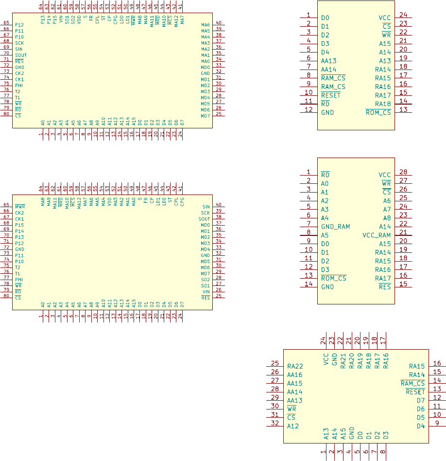
Bibliography
[1] “Microcomputers Data Book (1990).” Sharp Corporation. [Online]. Available: https://
archive.org/details/bitsavers_sharpdataBomputersDataBook_31076011
[2] “Microcomputer Data Book (1996).” Sharp Corporation. [Online]. Available: https://
archive.org/details/bitsavers_sharpdataBomputerDataBook_13840187
[3] “SM8311/SM8313/SM8314/SM8315 - 8-Bit Single-Chip Microcomputers (Controllers For
Home Appliances).” Sharp Corporation.
[4] Costis Sideris, “The quest for dumping GameBoy Boot ROMs!.” [Online]. Available: http://
www.its.caltech.edu/~costis/sgb_hack/
[5] gekkio, “Dumping the Super Game Boy 2 boot ROM.” [Online]. Available: https://gekkio.
fi/blog/2015/dumping-the-super-game-boy-2-boot-rom/
[6] Tauwasser, “MBC1 - Tauwasser's Wiki.” [Online]. Available: https://wiki.tauwasser.eu/view/
MBC1
[7] Pan of ATX, M. Fayzullin, P. Felber, P. Robson, and M. Korth, “Pan Docs - Everything
You Always Wanted To Know About GAMEBOY.” [Online]. Available: http://bgb.bircd.org/
pandocs.htm
[8] Tauwasser, “MBC2 - Tauwasser's Wiki.” [Online]. Available: https://wiki.tauwasser.eu/view/
MBC2
[9] Antonio Niño Díaz (AntonioND), “The Cycle-Accurate Game Boy Docs.” [Online]. Available:
https://github.com/AntonioND/giibiiadvance/tree/master/docs
[10] “Gameboy CPU (LR35902) instruction set.” [Online]. Available: http://www.pastraiser.com/
cpu/gameboy/gameboy_opcodes.html
168
